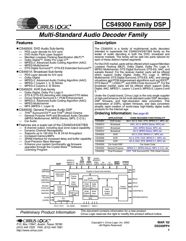
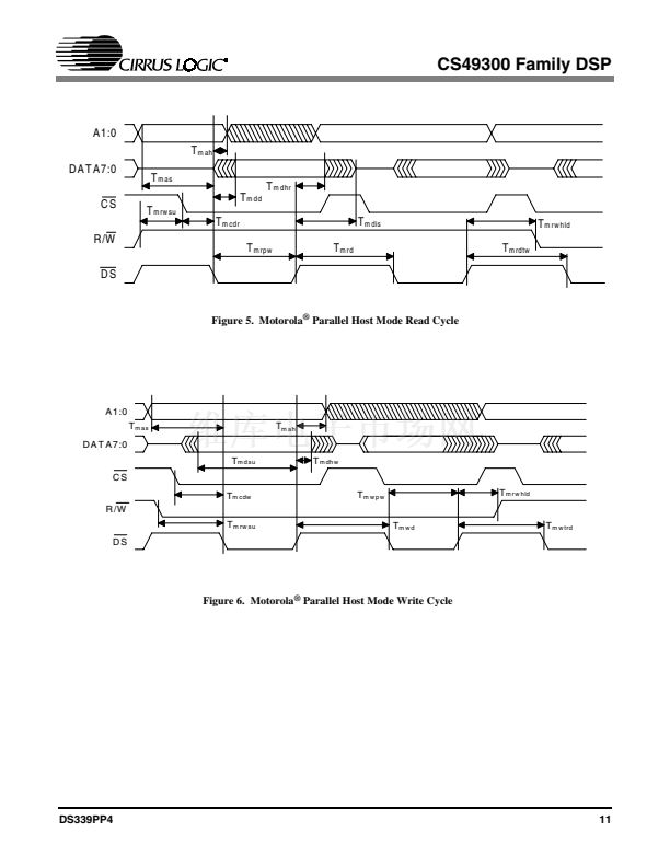
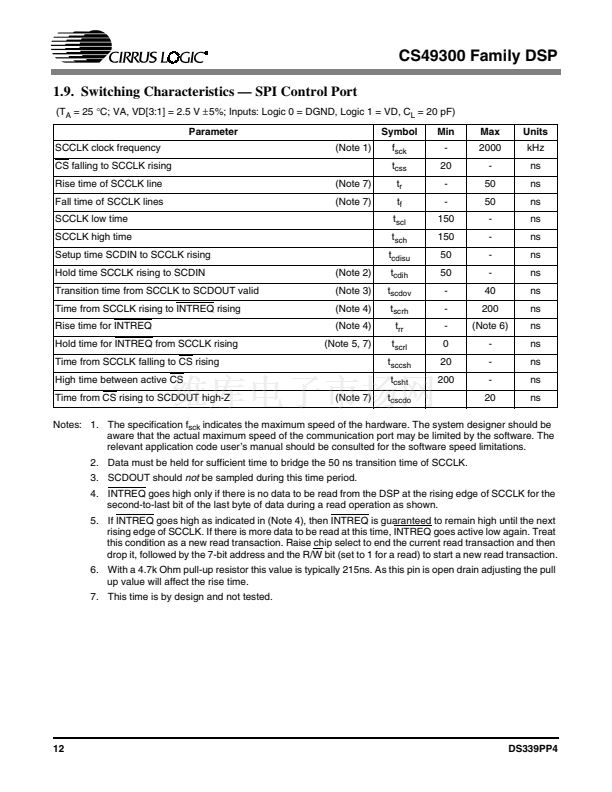
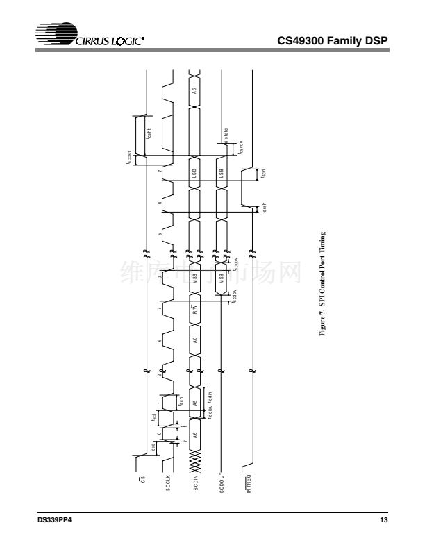
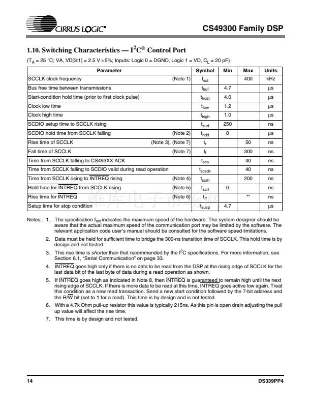
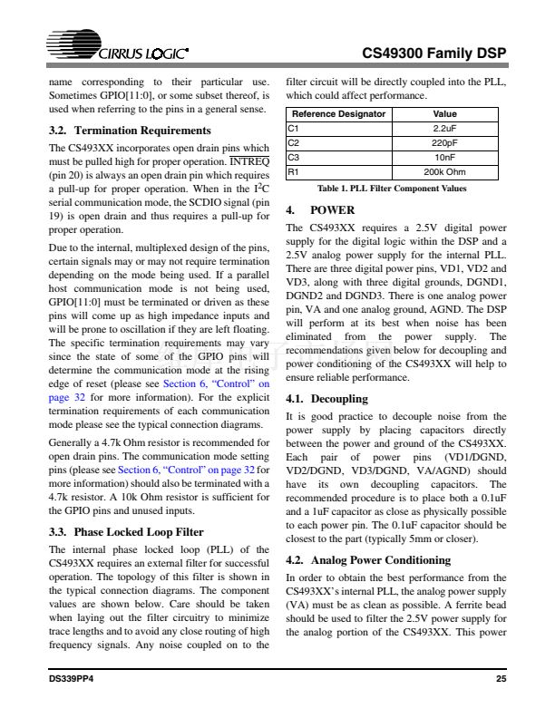
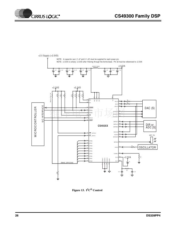
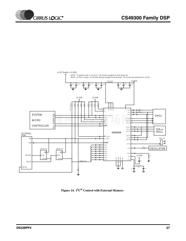
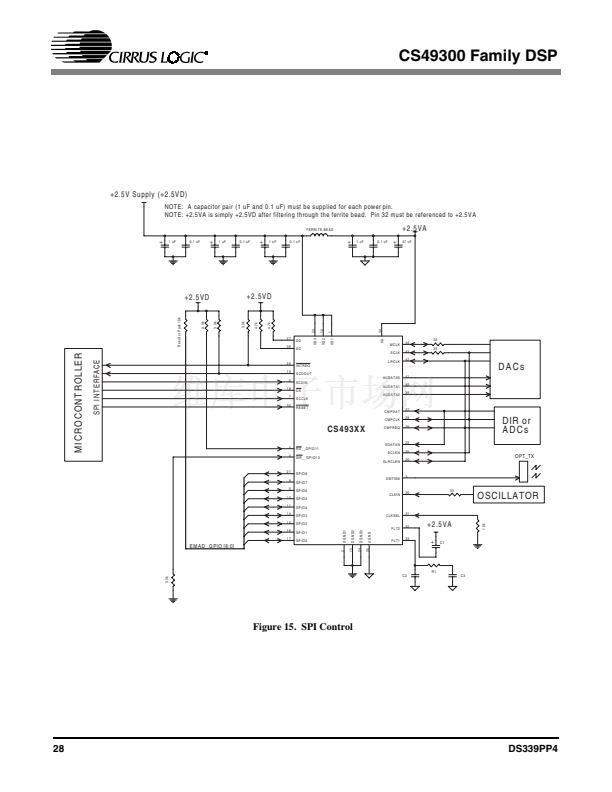
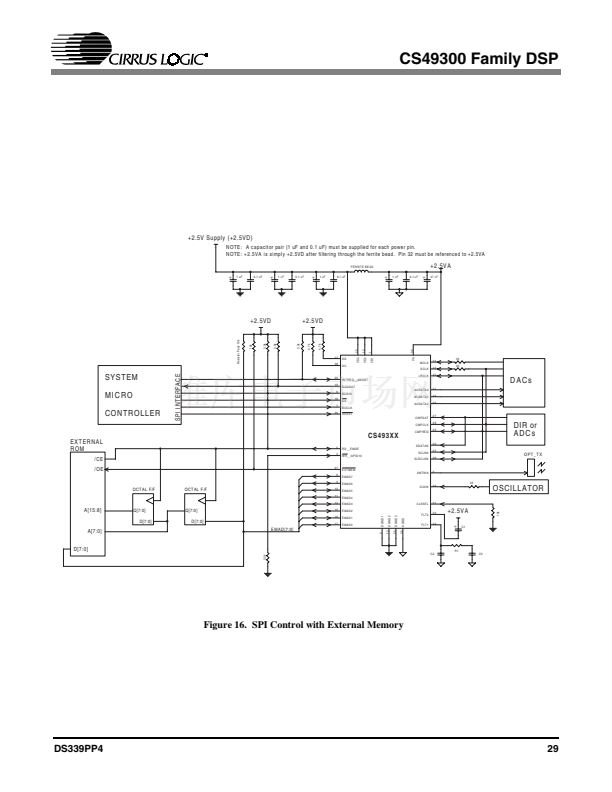
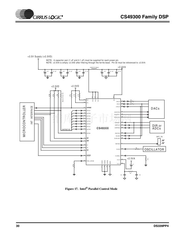
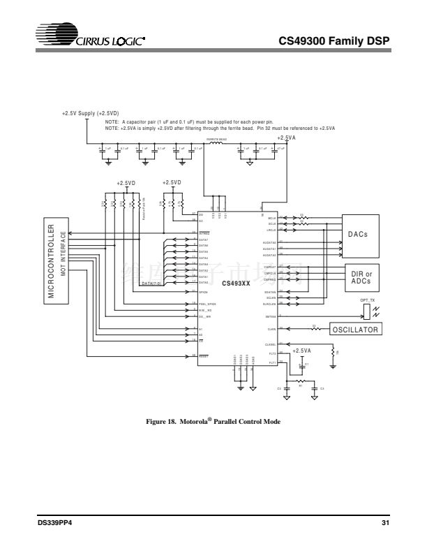
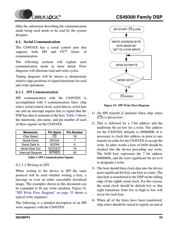
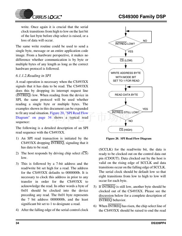
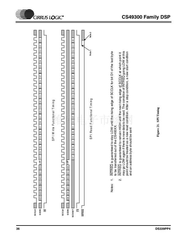
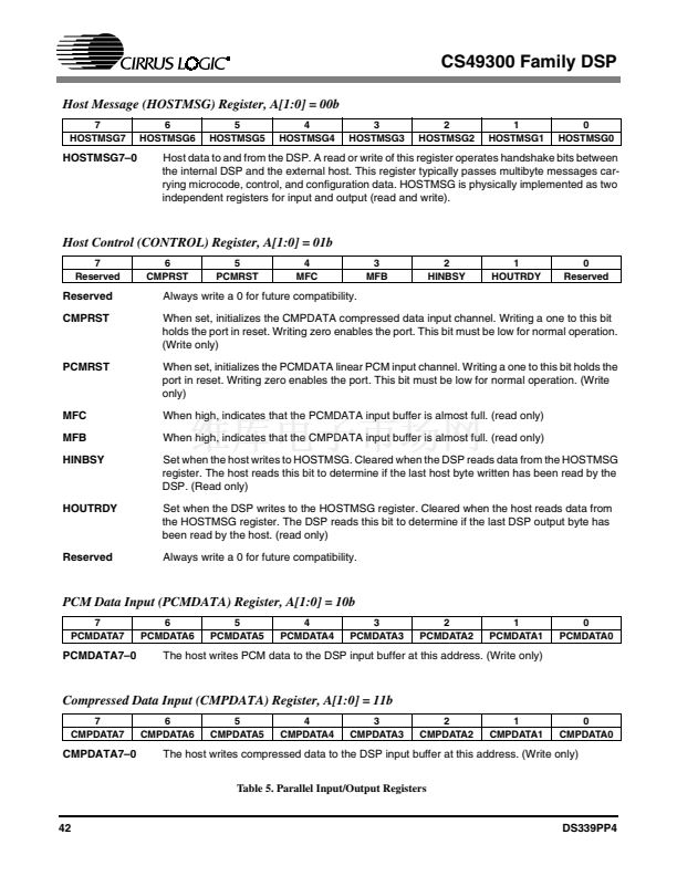
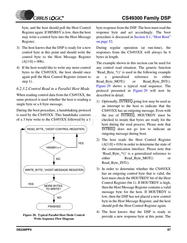
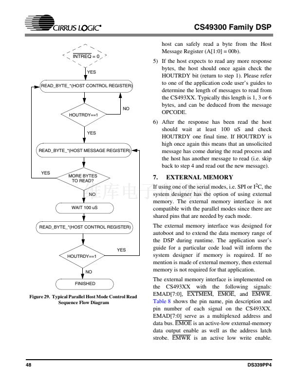
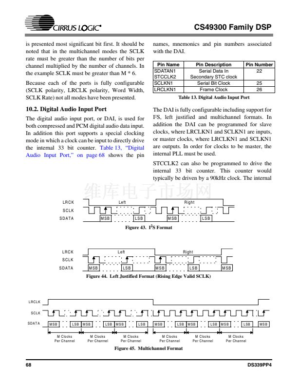
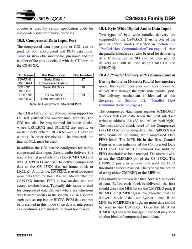
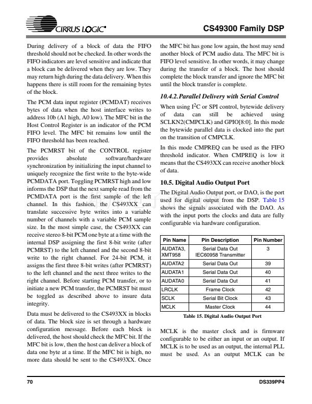
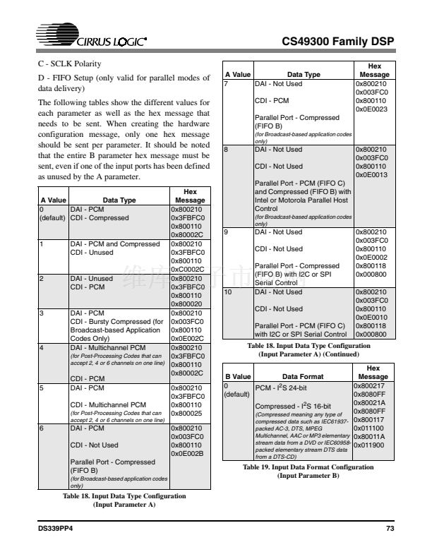
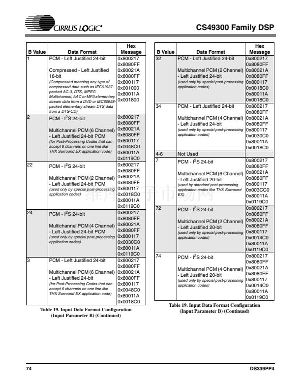
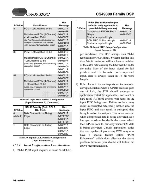
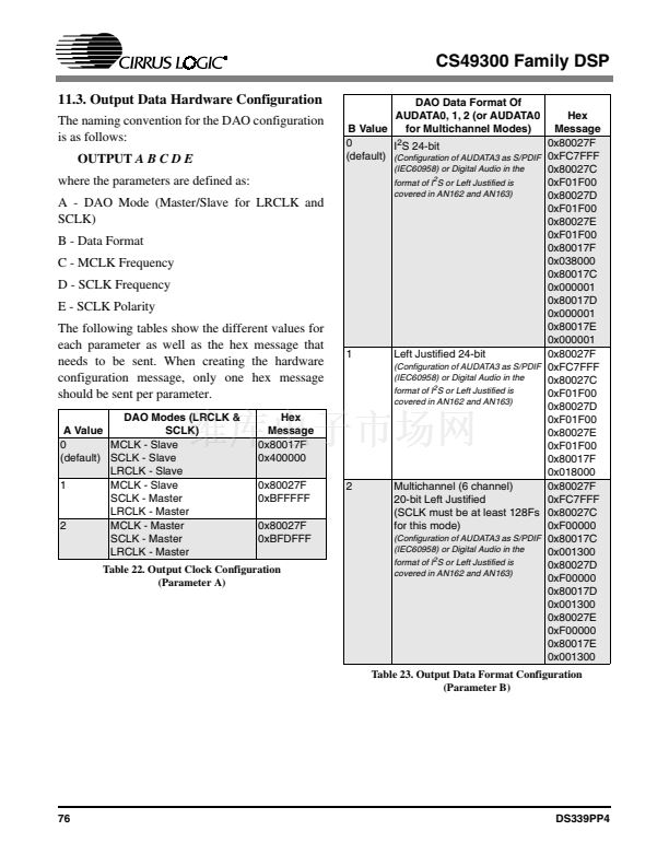
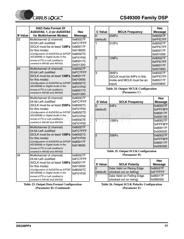
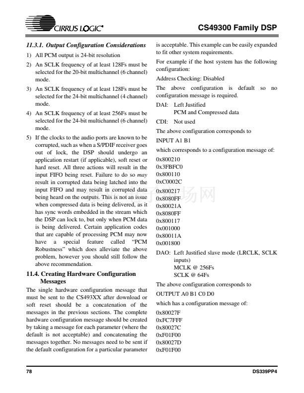
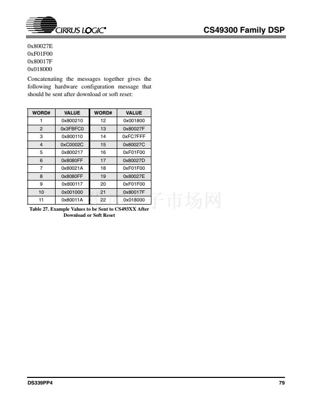
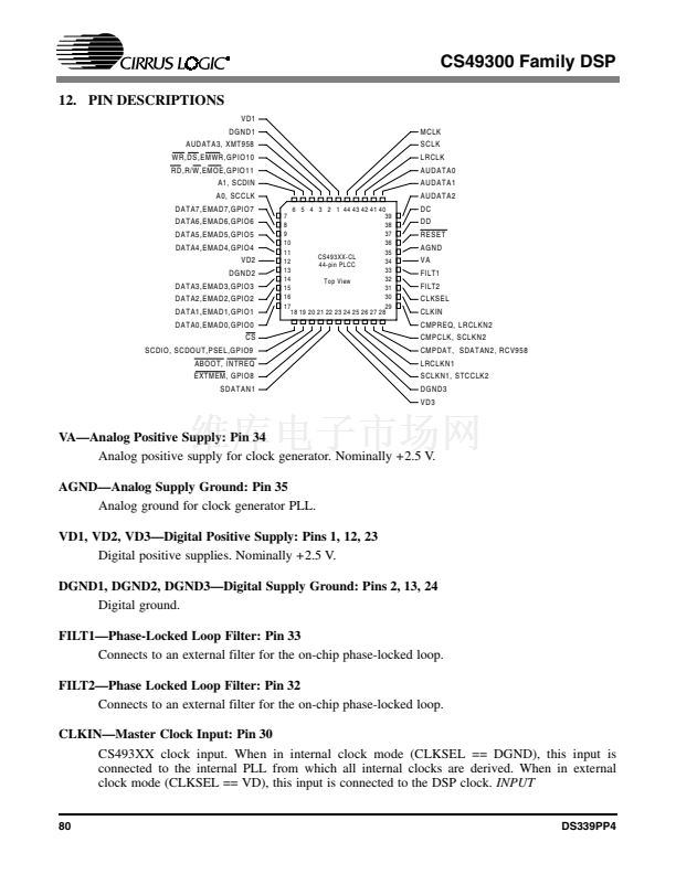
CS49300 Family DSP
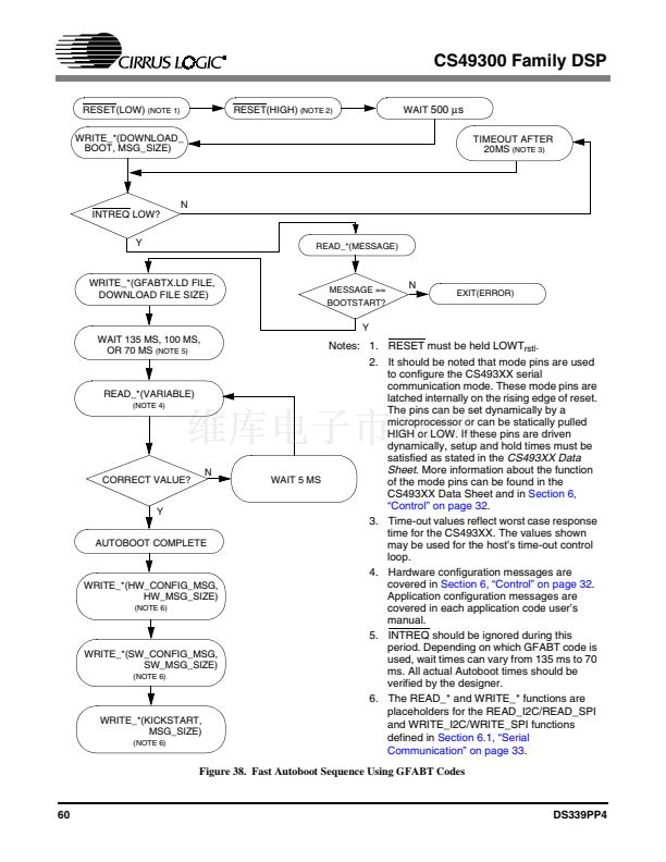
8.2. Autoboot
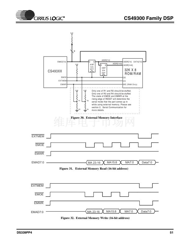
Autoboot is a feature available on all DSPs in the
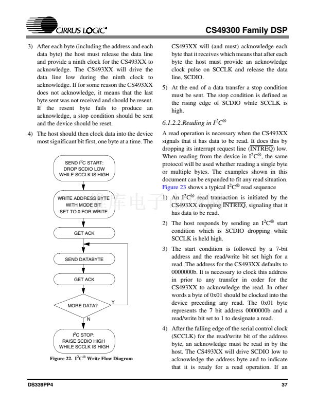
CS493XX family which gives the decoder the
ability to load application code into itself from an
external memory. Because external memory is
accessed through the external memory interface,
autoboot restricts the host control modes to serial
communication (I
2
C or SPI). For this section the
external memory interface shown in
Figure 30,
"External Memory Interface" on page 51
can be
referenced.
RESET and ABOOT are the control pins which are
used to initiate an autoboot operation by the host
controller. It is important to be aware that the
ABOOT pin also serves as the INTREQ pin, which
means that it will be driven by the CS493XX when
not in reset. Due to this constraint, ABOOT should
be connected to an open-drain output of the
microcontroller so as to allow the specified pull-up
resistor to generate a logic high level. At the
completion of a successful download, INTREQ
(ABOOT) becomes an output and the host should
no longer drive it.
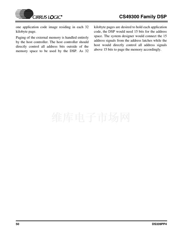
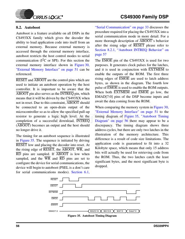
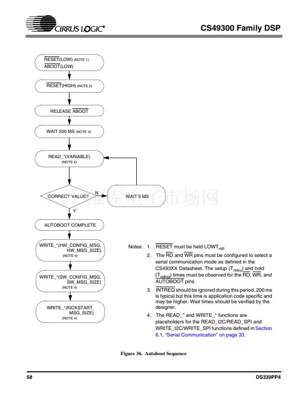
The timing for an autoboot sequence is illustrated
in
Figure 35.
The sequence is initiated by driving
RESET low and placing the decoder into reset. At
the rising edge of RESET, the ABOOT, WR, and
RD pins are sampled. If ABOOT is low when
sampled, and the WR and RD pins are set to
configure the device for serial communications, the
device will begin to autoboot (PSEL is a don鈥檛 care
for serial communications modes).
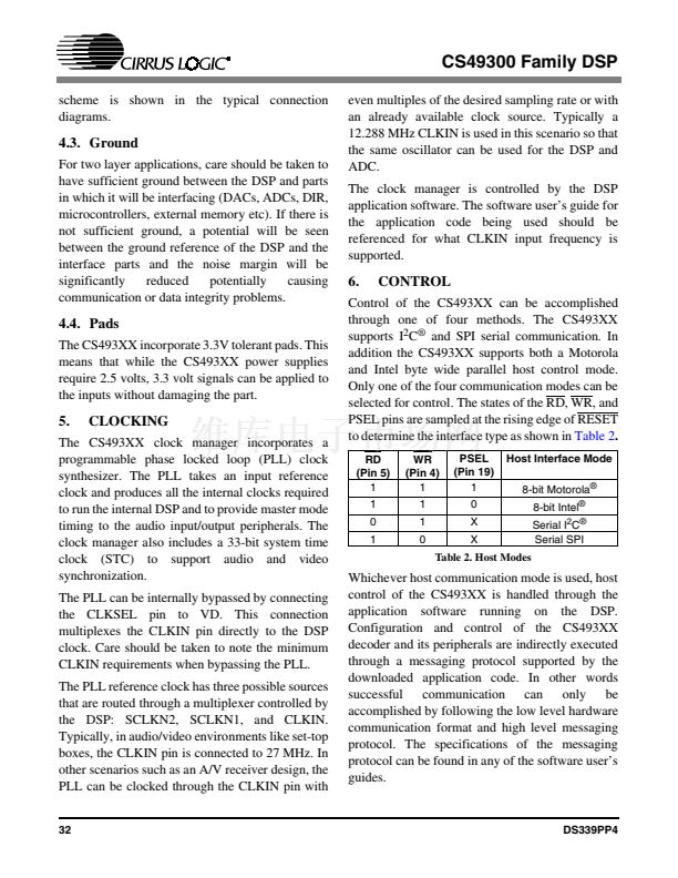
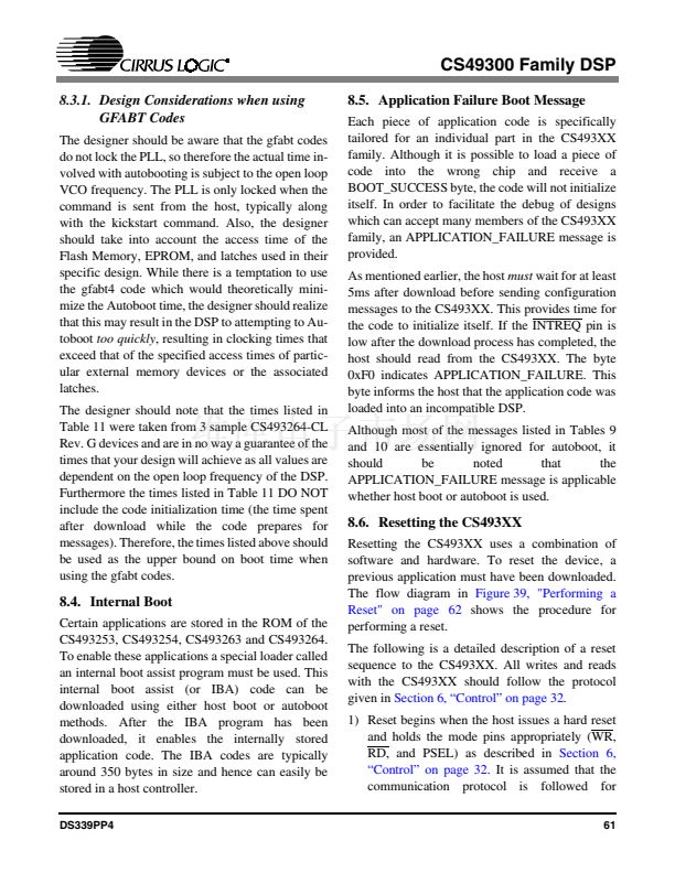
Section 6.1,
RE S E T
ABOOT
EXT M E M
EMOE
EMW R
E M A D7:0
M A 23:16
M A 15:8
M A 7:0
Data7:0
鈥淪erial Communication鈥?on page 33
discusses the
procedure required for placing the CS493XX into a
serial communication mode in more detail. For a
more thorough description of ABOOT鈥檚 behavior
after the rising edge of RESET please refer to
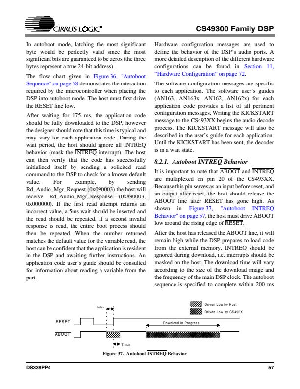
Section 8.2.1, 鈥淎utoboot INTREQ Behavior鈥?on
page 57
The EMOE pin of the CS493XX is used for two
purposes. It generates clock pulses for the latches,
and it is used in conjunction with EXTMEM to
enable the outputs of the ROM. The first three
rising edges of EMOE are used to latch address
bytes, as shown in the diagram. The fourth low
pulse of EMOE is used to enable the ROM outputs.
When both EXTMEM and EMOE go low, the
EMAD[7:0] pins of the DSP become inputs and
await the data coming from the ROM.
When comparing the memory system in
Figure 30,
"External Memory Interface" on page 51
to the
timing diagram of
Figure 35, "Autoboot Timing
Diagram" on page 56
there may appear to be a
discrepancy. The timing diagram shows three
address cycles, but there are only two latches in the
illustration of the memory architecture. This
difference is a result of code size limitations. The
application code is guaranteed to fit into a 32
Kilobyte space, which means that only 15 address
bits will actually be used for retrieving code from
the ROM. Thus, the two latches catch the least
significant bytes, and the most significant byte is
dropped.
Figure 35. Autoboot Timing Diagram
56
DS339PP4


 1
1
 2
2
 3
3
 4
4
 5
5
 6
6
 7
7
 8
8
 9
9
 10
10
 11
11
 12
12
 13
13
 14
14
 15
15
 16
16
 17
17
 18
18
 19
19
 20
20
 21
21
 22
22
 23
23
 24
24
 25
25
 26
26
 27
27
 28
28
 29
29
 30
30
 31
31
 32
32
 33
33
 34
34
 35
35
 36
36
 37
37
 38
38
 39
39
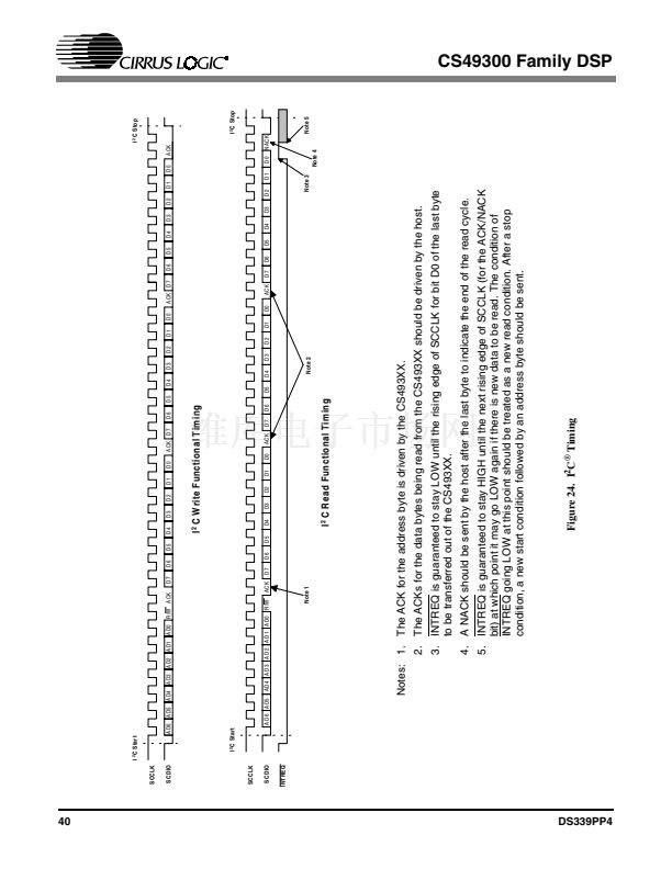 40
40
 41
41
 42
42
 43
43
 44
44
 45
45
 46
46
 47
47
 48
48
 49
49
 50
50
 51
51
 52
52
 53
53
 54
54
 55
55
 56
56
 57
57
 58
58
 59
59
 60
60
 61
61
 62
62
 63
63
 64
64
 65
65
 66
66
 67
67
 68
68
 69
69
 70
70
 71
71
 72
72
 73
73
 74
74
 75
75
 76
76
 77
77
 78
78
 79
79
 80
80
 81
81
 82
82
 83
83
 84
84
 85
85
 86
86
