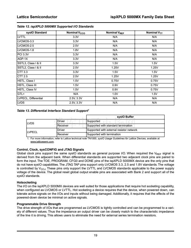
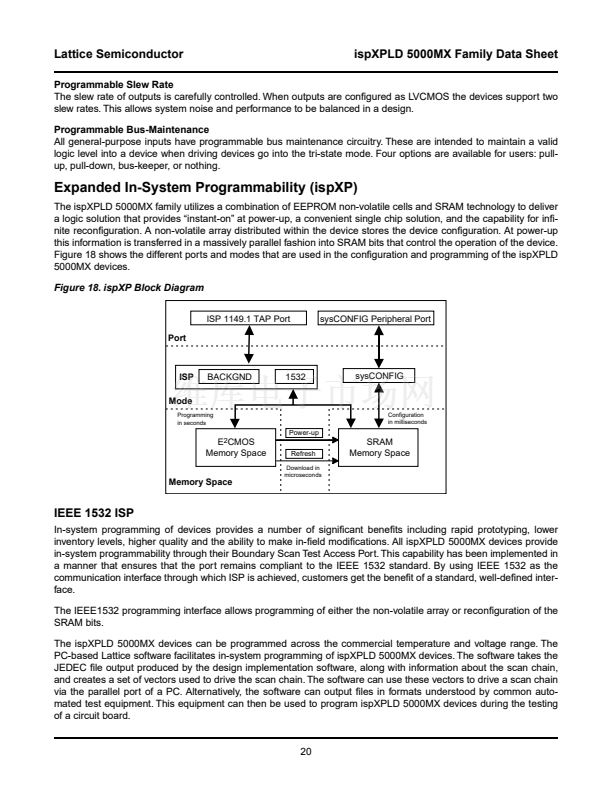
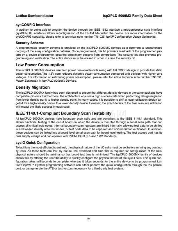
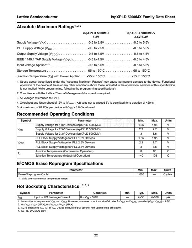
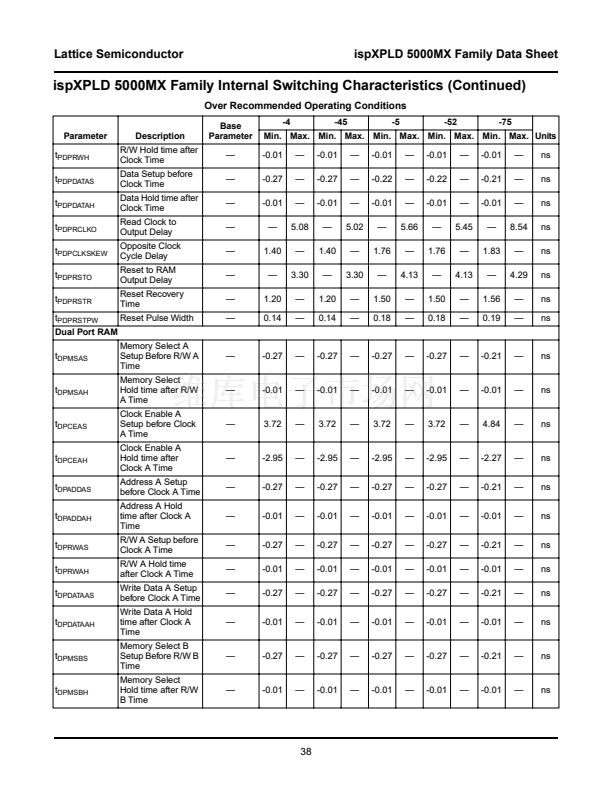
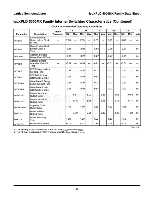
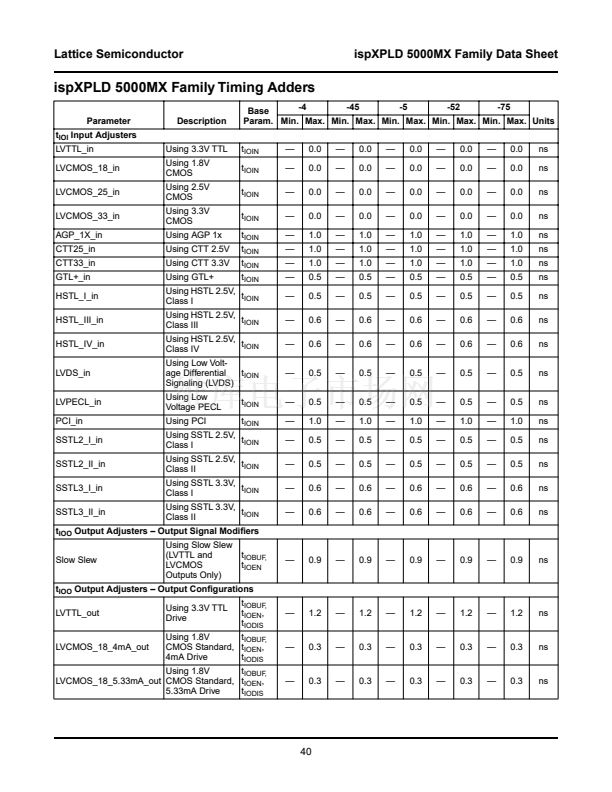
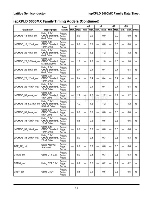
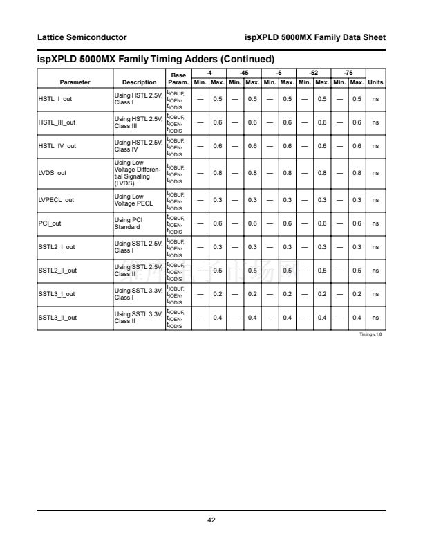
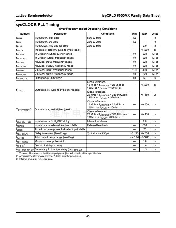
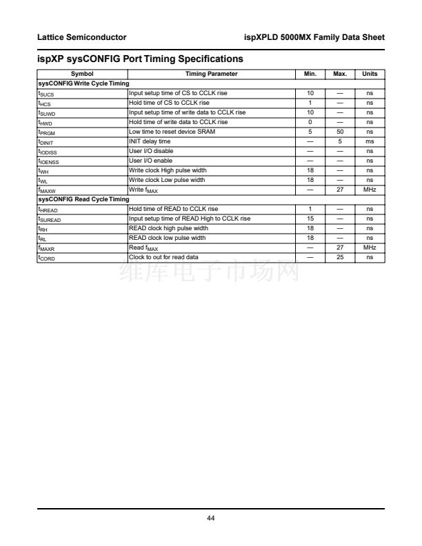
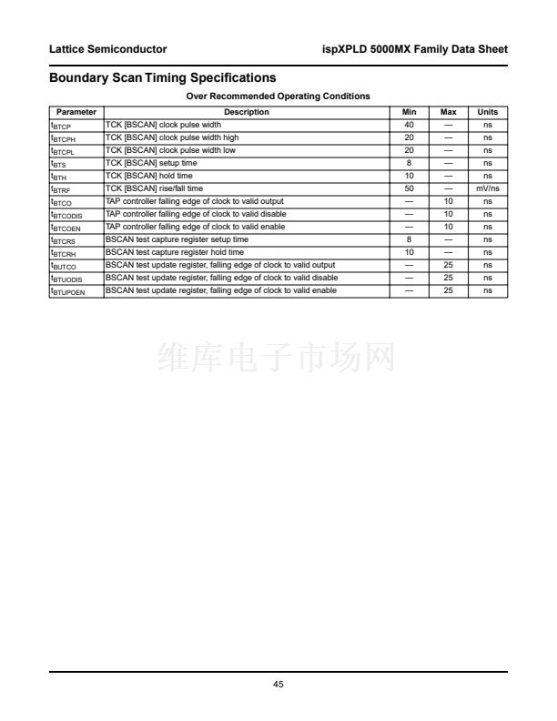
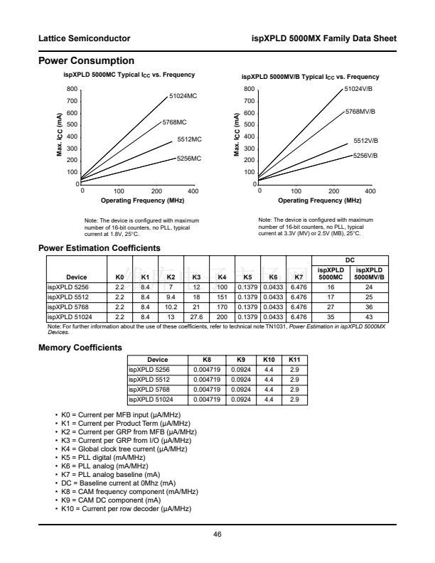
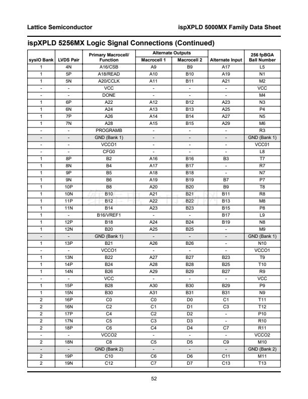
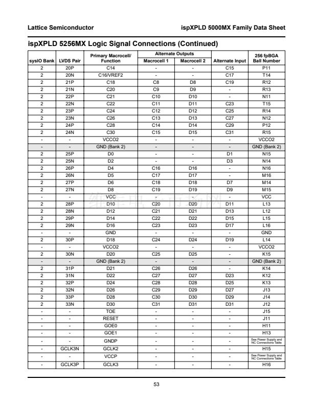
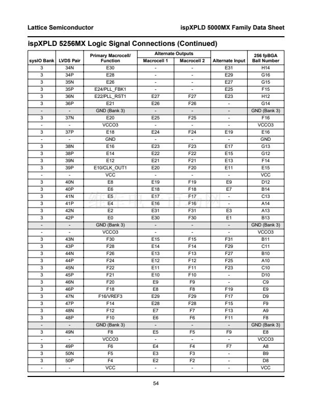
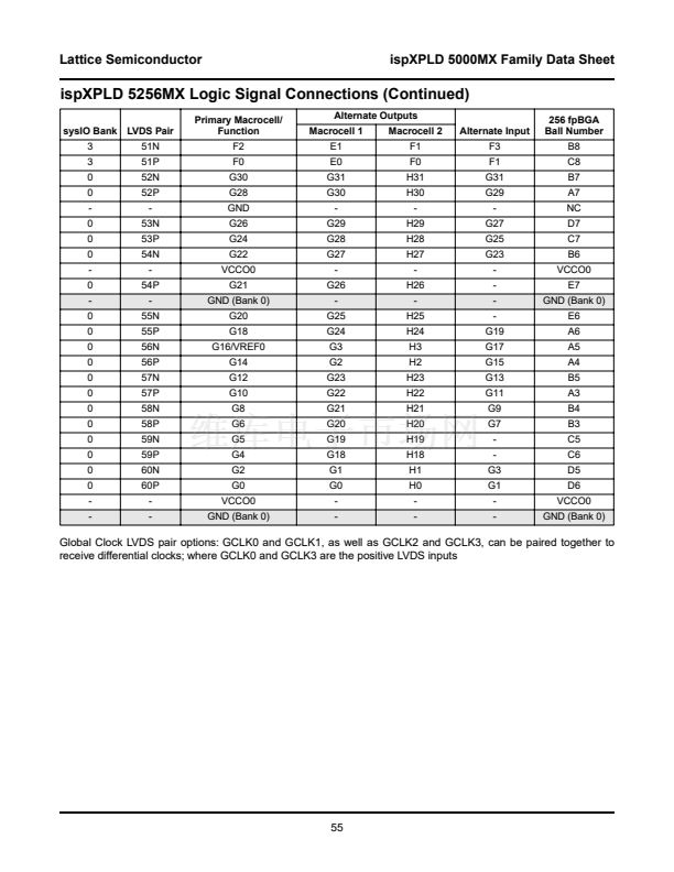
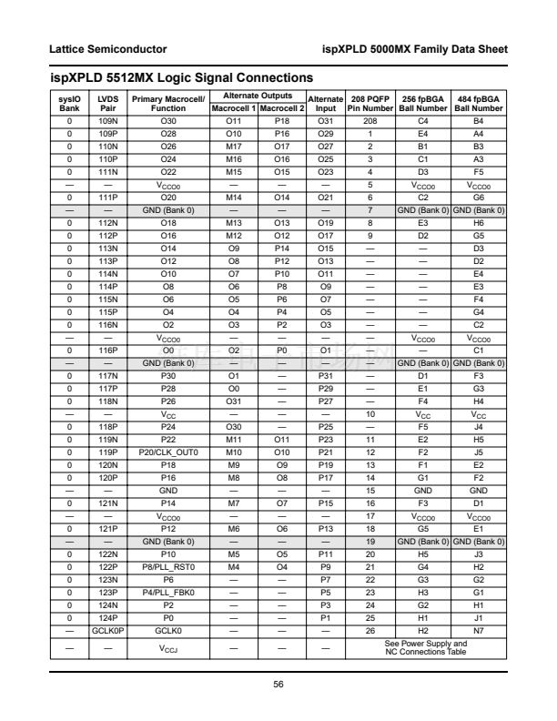
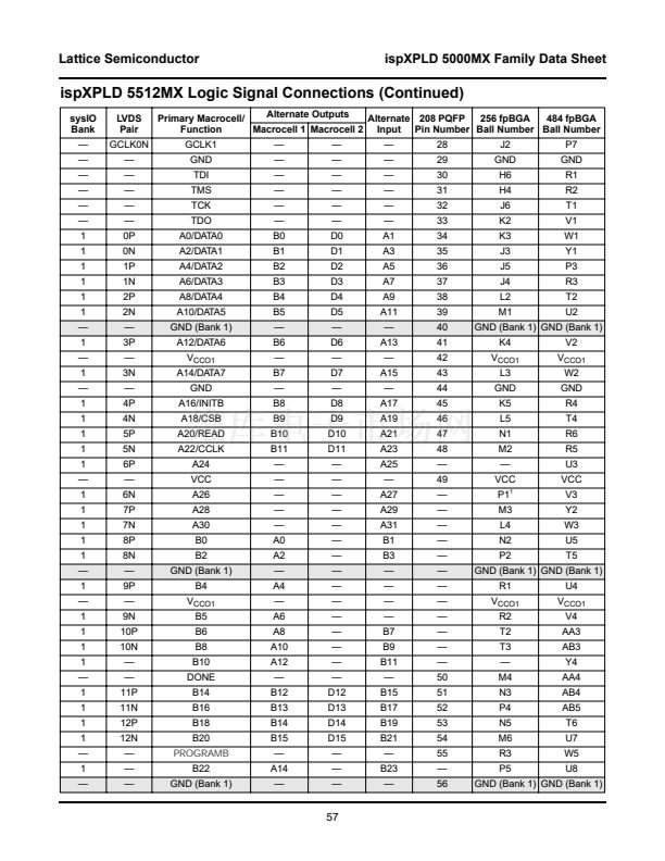
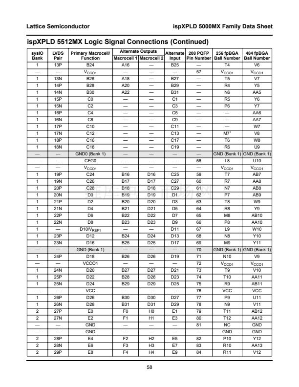
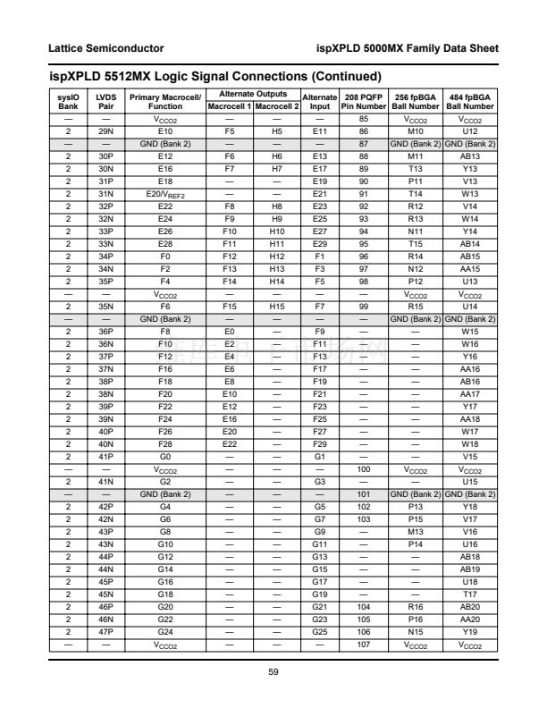
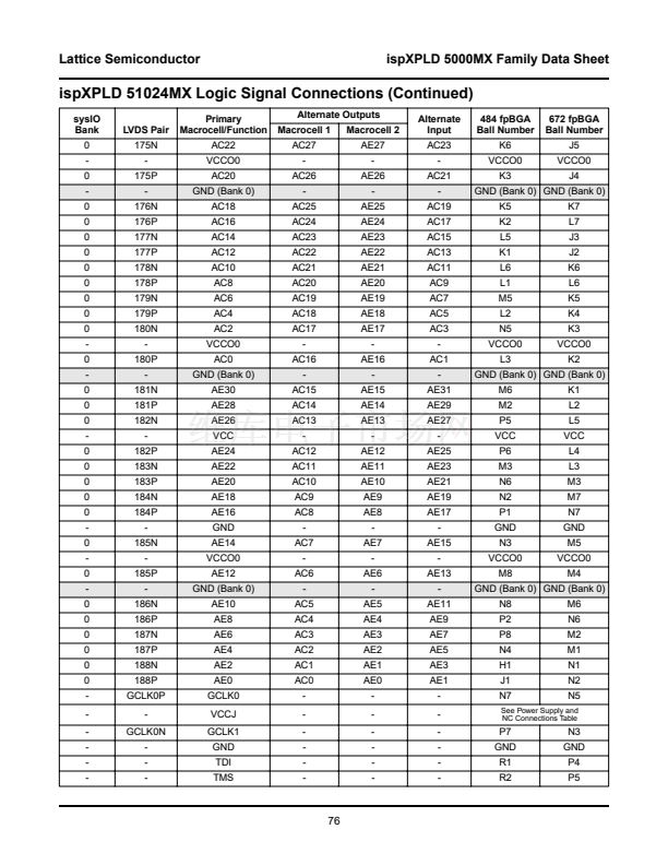
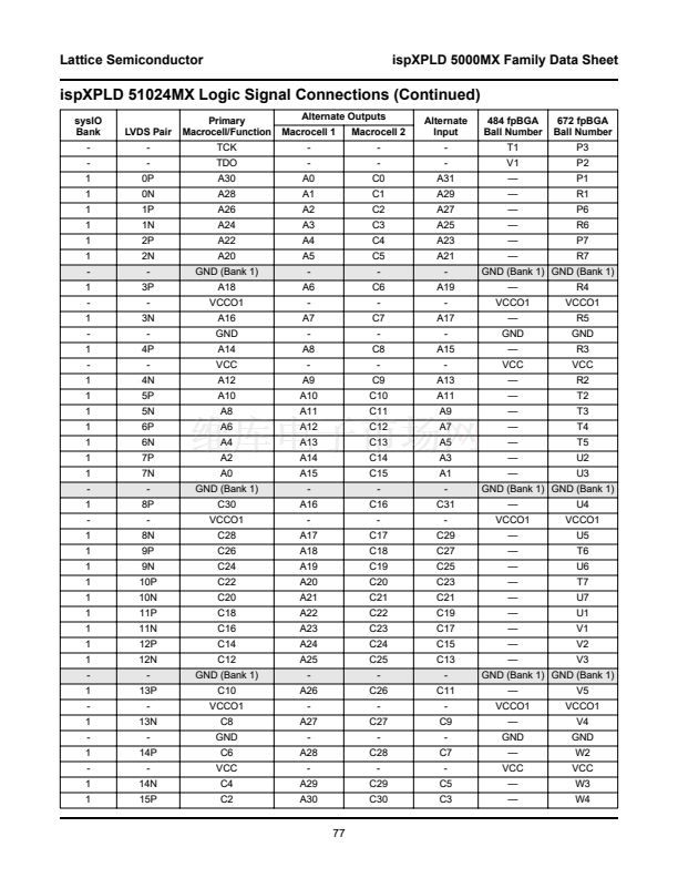
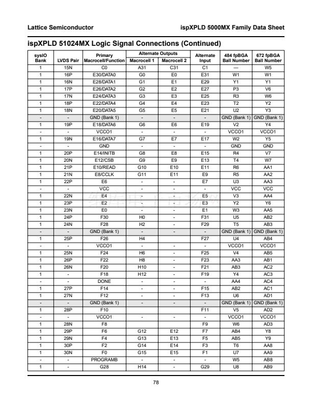
Lattice Semiconductor
Pseudo Dual-Port SRAM Mode
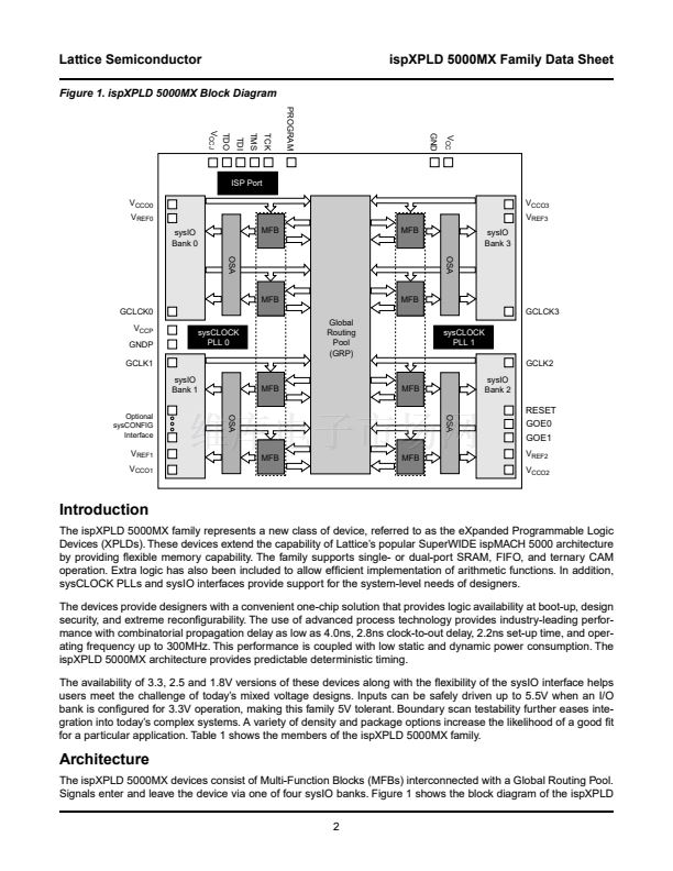
ispXPLD 5000MX Family Data Sheet
In Pseudo Dual-Port SRAM Mode the multi-function array is con铿乬ured as a SRAM with an independent read and
write ports that access the same 16,384-bits of memory. Data widths of 1, 2, 4, 8, 16 and 32 are supported by the
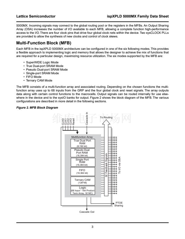
MFB. Figure 10 shows the block diagram of the Pseudo Dual-Port SRAM.
Write data, write address, chip select and write enable signals are always synchronous (registered). The read data
and read address signals can be synchronous or asynchronous. Reset is asynchronous. All write signals share the
same clock, and clock enable. All read signals share the same clock and clock enable. Reset is shared by both
read and write signals. Table 6 shows the possible sources for the clock, clock enable and initialization signals for
the various registers.
Figure 10. Pseudo Dual-Port SRAM Block Diagram
CLK0
CLK1
CLK2
CLK3
RESET
Read Address
(RAD[0:8-13])
Read Data
(RD[0:0-15])
Write Address
(WAD[0:8-13])
68 Inputs
From
Routing
16,384 bit
Pseudo
鈥?/div>
Dual
Write Enable
(WE)
鈥?/div>
Port
Write Clock
(WCLK)
SRAM
Write Chip Sel
(WCS[0,1])
Array
(WD[0:0,1,3,7,15,31])
Write Data
Write Clk Enable
(WCEN)
Read Clk Enable
(RCEN)
Read Clock
(RCLK)
Reset
(RST)
Table 6. Register Clock, Clock Enable, and Reset in Pseudo Dual-Port SRAM Mode
Register
Input
Clock
Write Address, Write
Clock Enable
Data, Write Enable,
and Write Chip Select
Reset
Clock
Read Data and Read Clock Enable
Address
Reset
Source
WCLK or one of the global clocks (CLK0 - CLK3). The selected signal can
be inverted if desired.
WCEN or one of the global clocks (CLK1 - CLK2). The selected signal can
be inverted if desired.
Created by the logical OR of the global reset signal and RST. RST may have
inversion if desired.
RCLK or one of the global clocks (CLK0 - CLK3). The selected signal can be
inverted if desired.
RCEN or one of the global clocks (CLK1 - CLK2). The selected signal can
be inverted if desired.
Created by the logical OR of the global reset signal and RST. RST may have
inversion if desired.
11


 1
1
 2
2
 3
3
 4
4
 5
5
 6
6
 7
7
 8
8
 9
9
 10
10
 11
11
 12
12
 13
13
 14
14
 15
15
 16
16
 17
17
 18
18
 19
19
 20
20
 21
21
 22
22
 23
23
 24
24
 25
25
 26
26
 27
27
 28
28
 29
29
 30
30
 31
31
 32
32
 33
33
 34
34
 35
35
 36
36
 37
37
 38
38
 39
39
 40
40
 41
41
 42
42
 43
43
 44
44
 45
45
 46
46
 47
47
 48
48
 49
49
 50
50
 51
51
 52
52
 53
53
 54
54
 55
55
 56
56
 57
57
 58
58
 59
59
 60
60
 61
61
 62
62
 63
63
 64
64
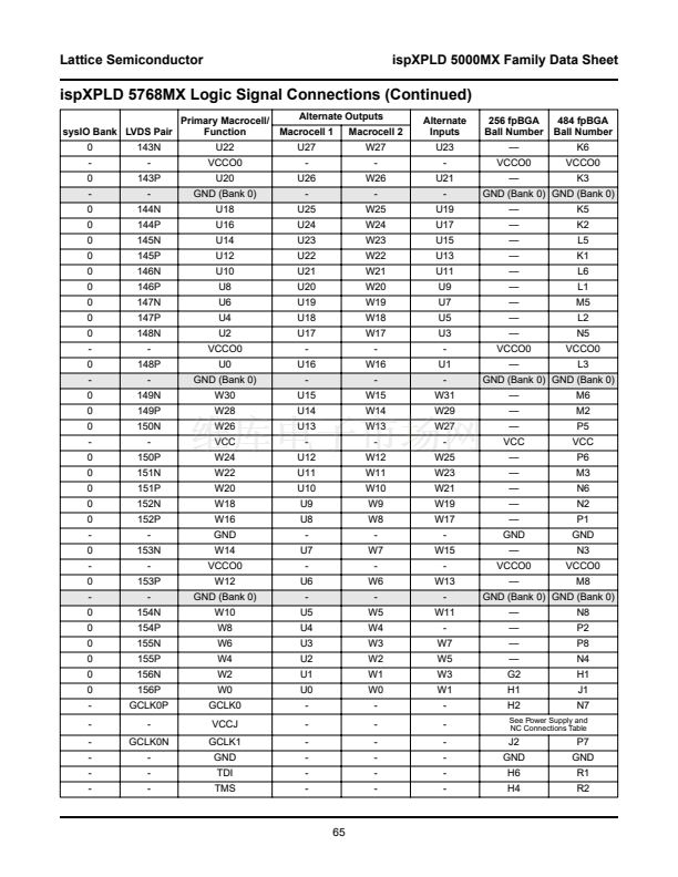 65
65
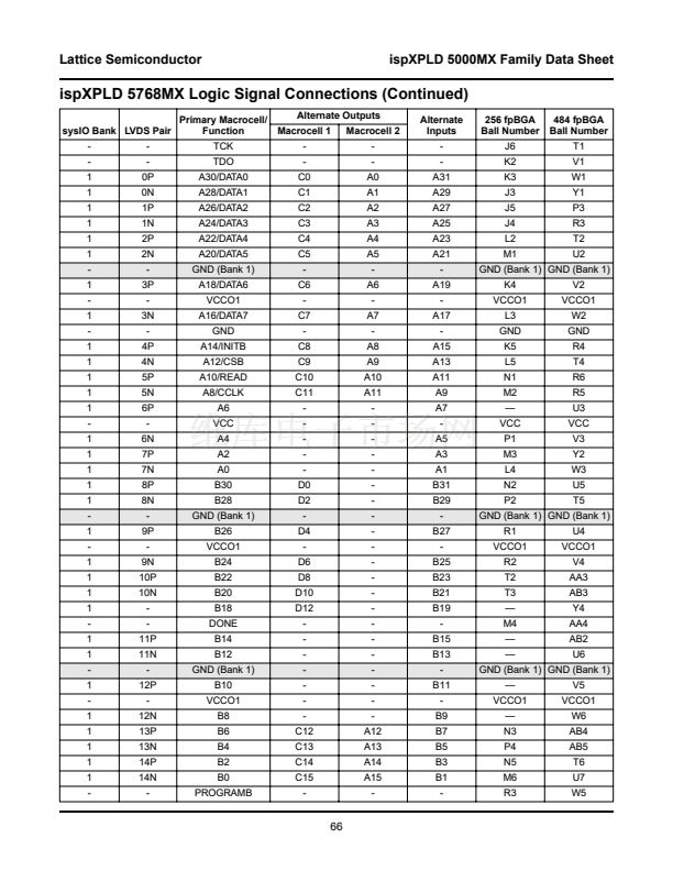 66
66
 67
67
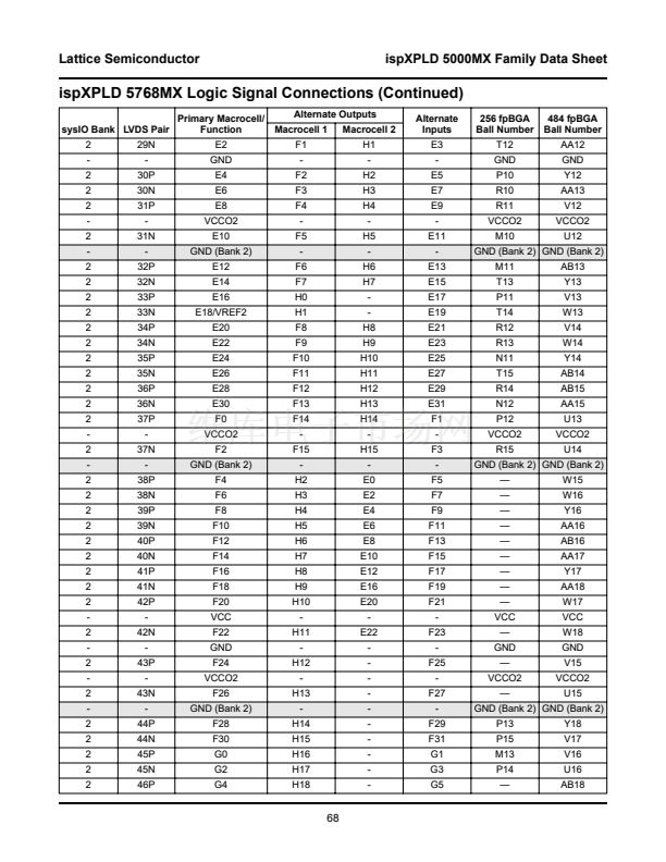 68
68
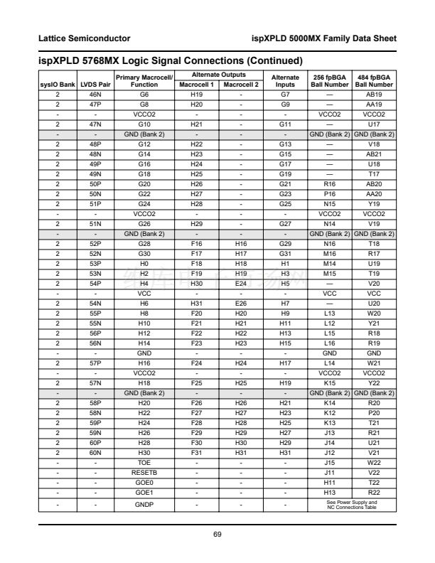 69
69
 70
70
 71
71
 72
72
 73
73
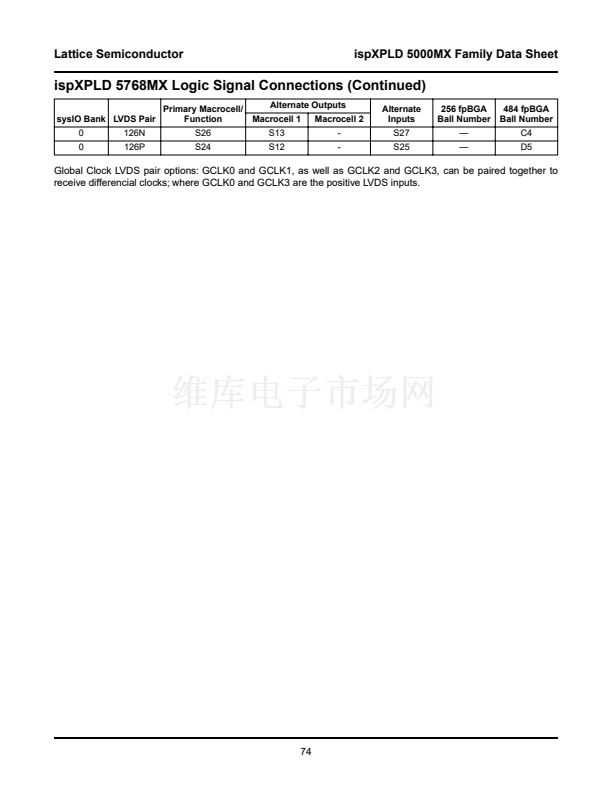 74
74
 75
75
 76
76
 77
77
 78
78
 79
79
 80
80
 81
81
 82
82
 83
83
 84
84
 85
85
 86
86
 87
87
 88
88
 89
89
 90
90
 91
91
 92
92
