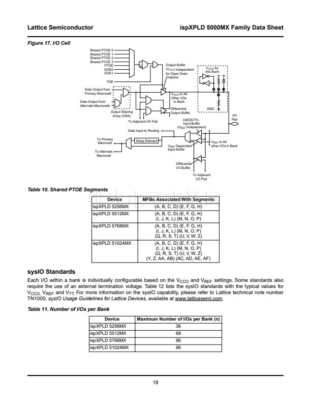
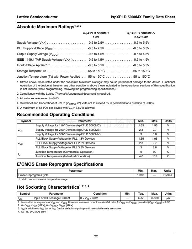
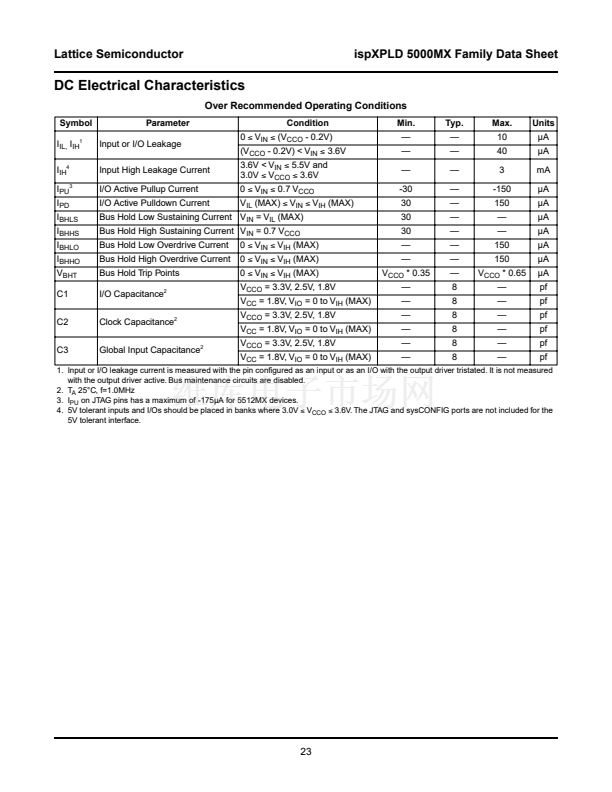
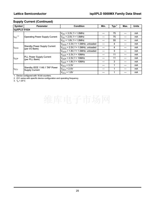
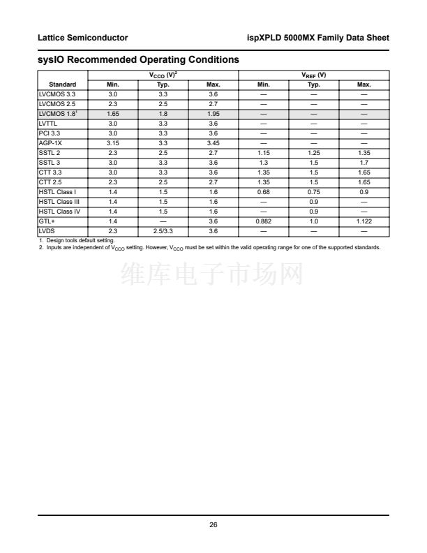
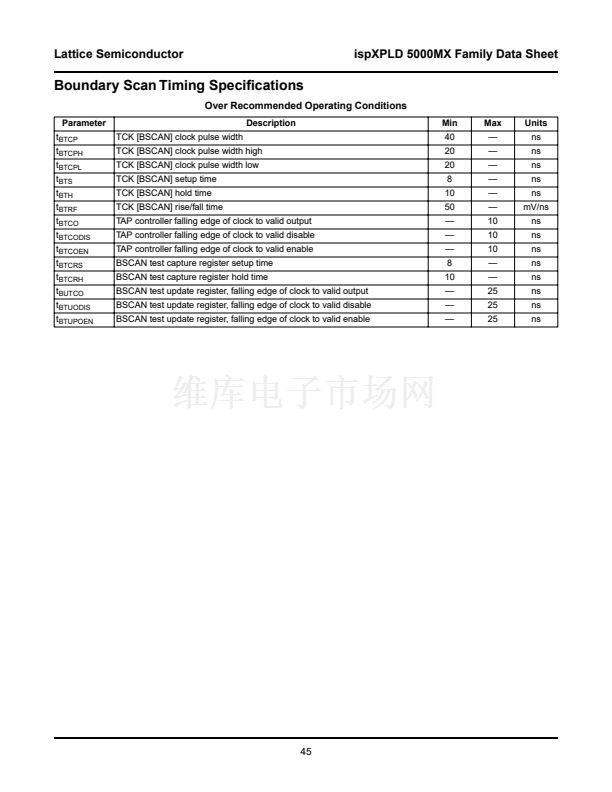
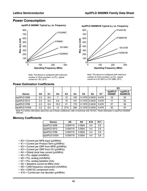
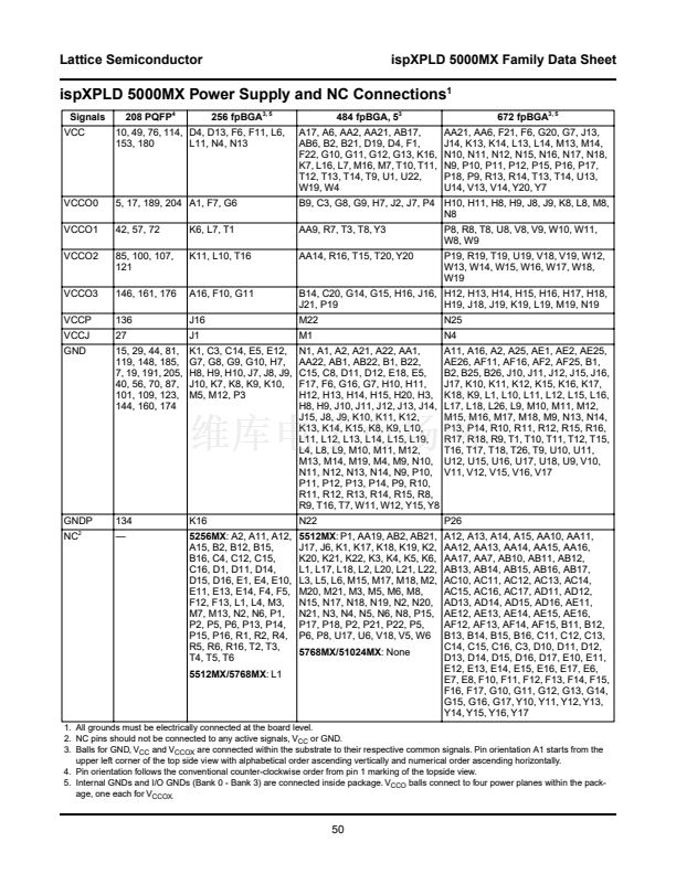
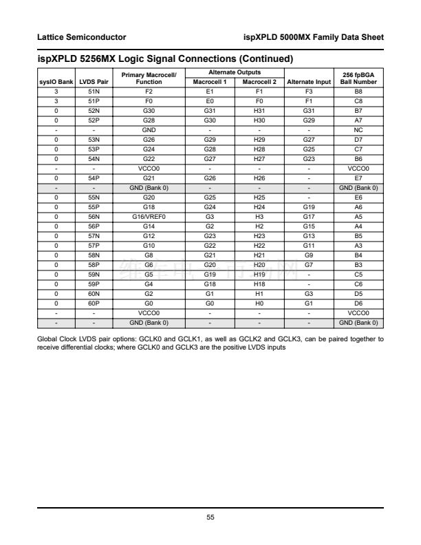
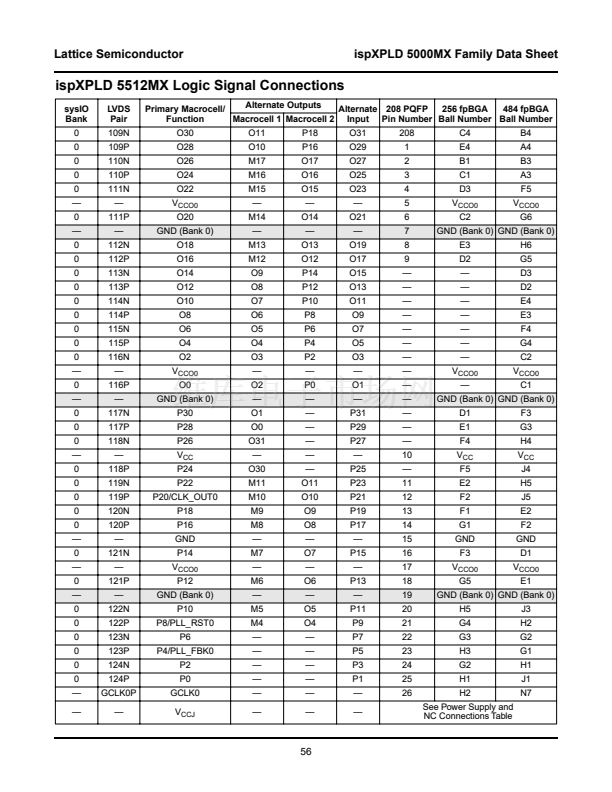
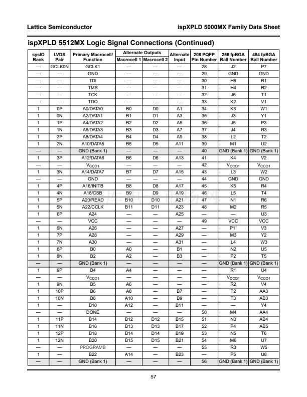
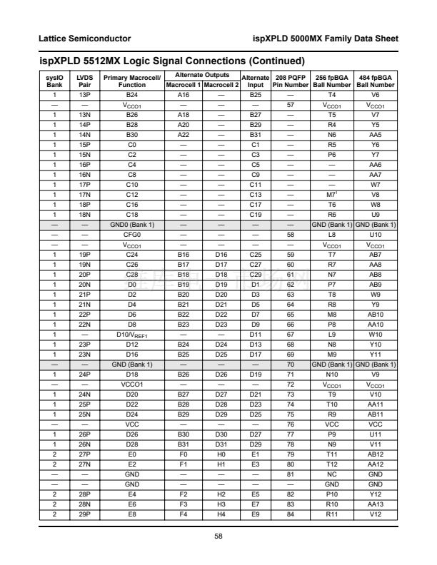
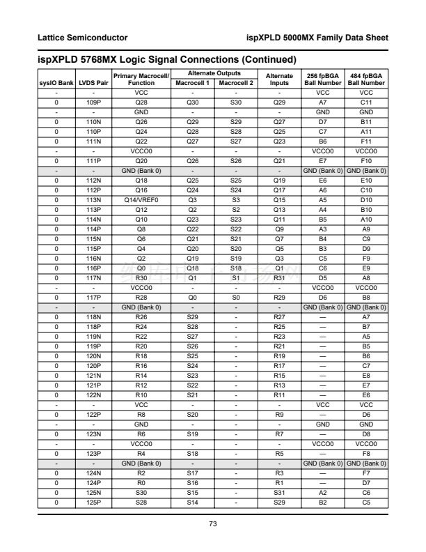
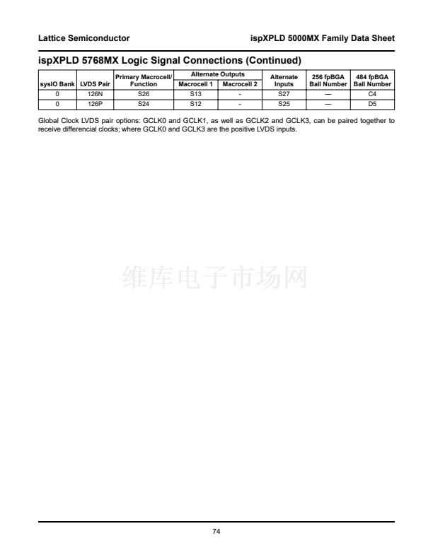
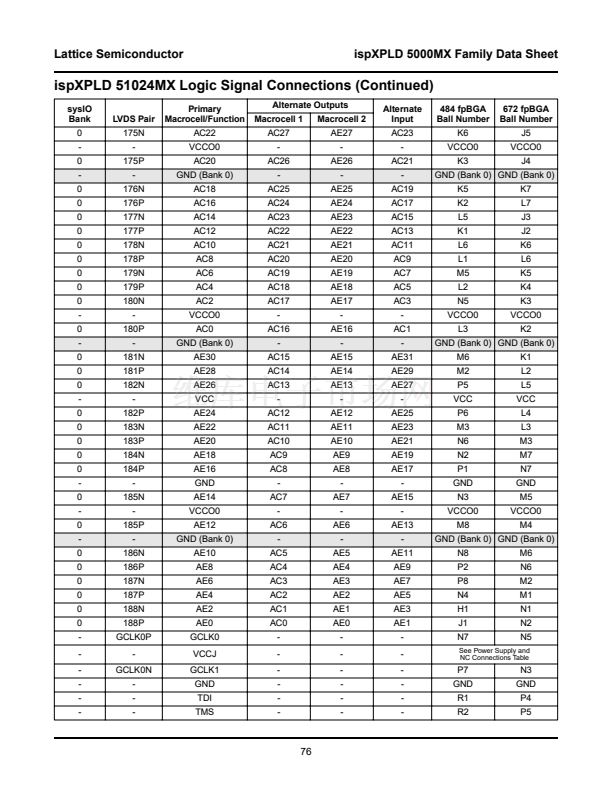
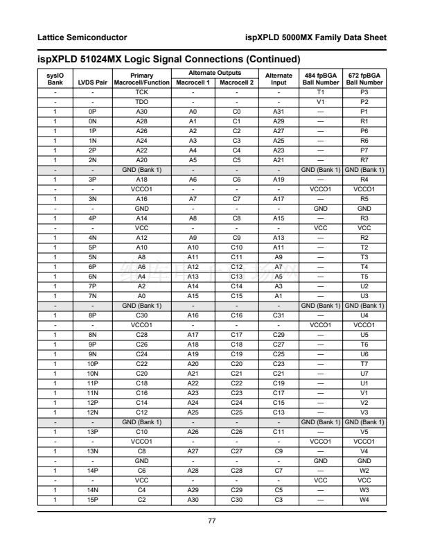
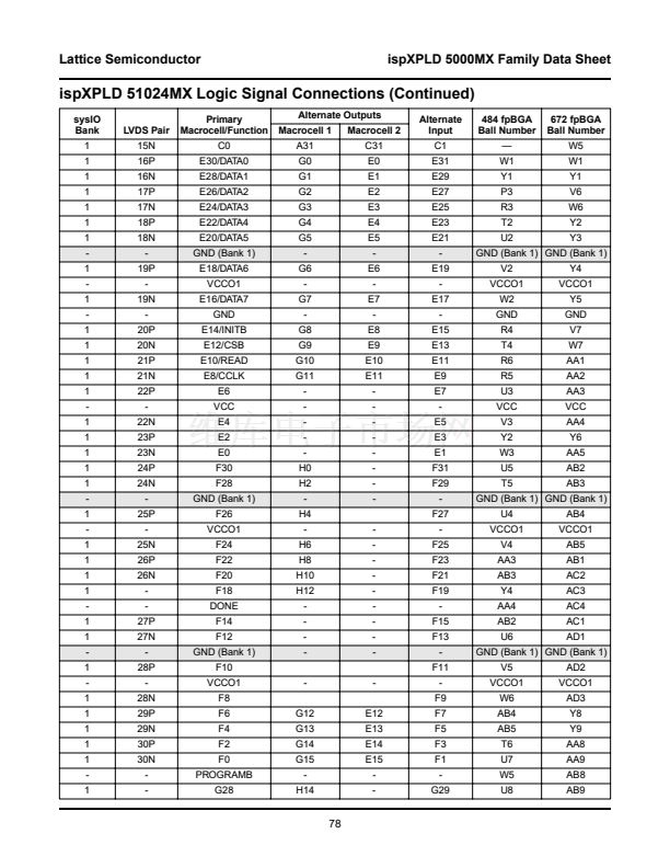
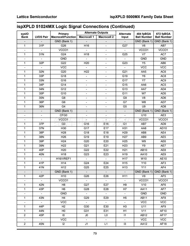
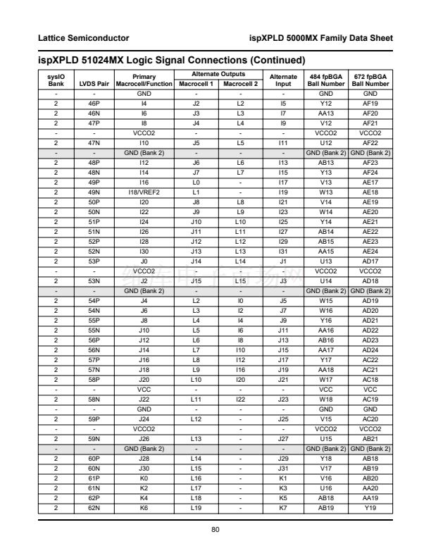
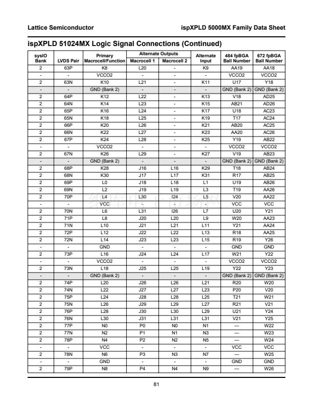
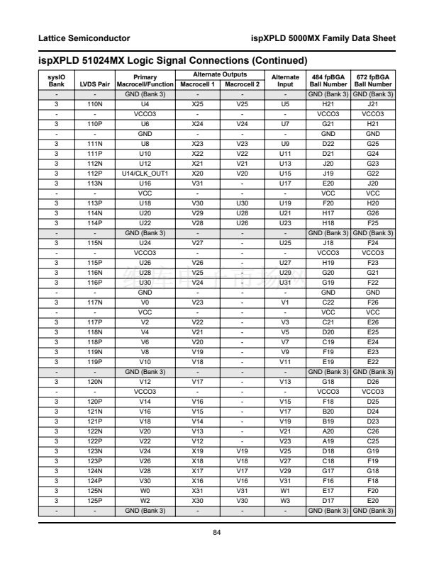
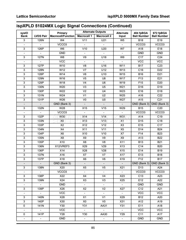
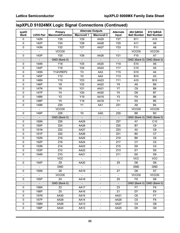
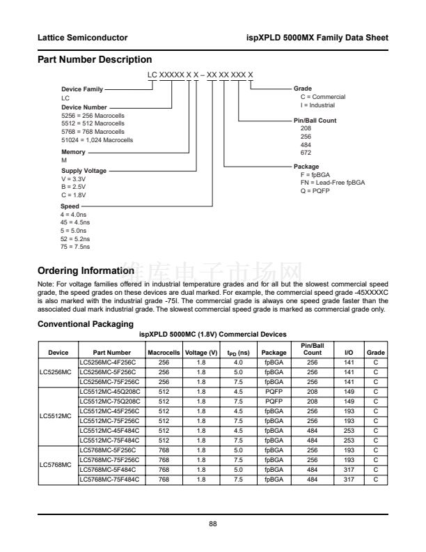
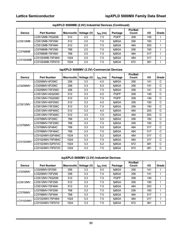
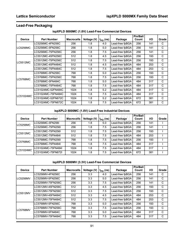
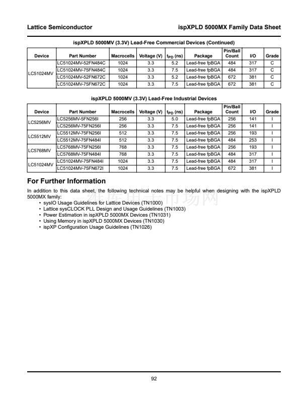
Lattice Semiconductor
FIFO Mode
ispXPLD 5000MX Family Data Sheet
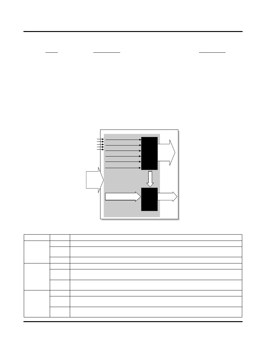
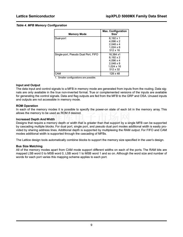
In FIFO Mode the multi-function array is con铿乬ured as a FIFO (First In First Out) buffer with built in control. The
read and write clocks can be different or the same dependent on the application. Four 铿俛gs show the status of the
FIFO; Full, Empty, Almost Full, and Almost Empty. The thresholds for Full, Almost full and Almost empty are pro-
grammable by the user. It is possible to reset the read pointer, allowing support of frame retransmit in communica-
tions applications. If desired, the block can be used in show ahead mode allowing the early reading of the next read
address.
In this mode one ports accesses 16,384-bits of memory. Data widths of 1, 2, 4, 8, 16 and 32 are supported by the
MFB. Figure 12 shows the block diagram of the FIFO.
Write data, write enable, 铿俛g outputs and read enable are synchronous. The Write Data, Almost Full and Full share
the same clock and clock enables. Read outputs are synchronous although these can be con铿乬ured in look ahead
mode. The Read Data, Empty and Almost Empty signals share the same clock and clock enables. Reset is shared
by all signals. Table 8 shows the possible sources for the clock, clock enable and reset signals for the various reg-
isters.
Figure 12. FIFO Block Diagram
Write Enable
(WE)
Write Clock
(WCLK)
Reset
(RST)
CLK0
CLK1
CLK2
CLK3
RESET
Read Clock
(RCLK)
Reset_RP
(RSTRP)
FIFO
Control
Logic
FIFO
Flags*
Full,
Empty,
Almost Full,
Almost Empty
Read Enable
(RE)
鈥?/div>
鈥?/div>
68 Inputs
From
Routing
Write Data
(DI[0:0-31])
16,384-bit
Read Data
(DO[0:0-31])
SRAM
Array
*Control logic can be
duplicated in adjacent MFB
in 32-bit mode
Table 8. Register Clocks, Clock Enables, and Initialization in FIFO Mode
Register
Input
Source
WCLK or one of the global clocks (CLK0 - CLK3). Each of these signals can be inverted if required.
WE or one of the global clocks (CLK1 - CLK 2). Each of these signals can be inverted if required.
N/A
WCLK or one of the global clocks (CLK0 - CLK3). Each of these signals can be inverted if required.
WE or one of the global clocks (CLK1 - CLK 2). Each of these signals can be inverted if required.
Created by the logical OR of the global reset signal and RST. RST is routed by the multifunction
array from GRP, with inversion if desired.
RCLK or one of the global clocks (CLK0 - CLK3). Each of these signals can be inverted if required.
RE or one of the global clocks (CLK1 - CLK 2). Each of these signals can be inverted if required.
Created by the logical OR of the global reset signal and RST. RST is routed by the multifunction
array from GRP, with inversion if desired.
Write Data,
Clock
Write Enable Clock
Enable
Reset
Full and
Almost Full
Flags
Clock
Clock
Enable
Reset
Read Data,
Clock
Empty and
Clock
Almost Empty Enable
Flags
Reset
13


 1
1
 2
2
 3
3
 4
4
 5
5
 6
6
 7
7
 8
8
 9
9
 10
10
 11
11
 12
12
 13
13
 14
14
 15
15
 16
16
 17
17
 18
18
 19
19
 20
20
 21
21
 22
22
 23
23
 24
24
 25
25
 26
26
 27
27
 28
28
 29
29
 30
30
 31
31
 32
32
 33
33
 34
34
 35
35
 36
36
 37
37
 38
38
 39
39
 40
40
 41
41
 42
42
 43
43
 44
44
 45
45
 46
46
 47
47
 48
48
 49
49
 50
50
 51
51
 52
52
 53
53
 54
54
 55
55
 56
56
 57
57
 58
58
 59
59
 60
60
 61
61
 62
62
 63
63
 64
64
 65
65
 66
66
 67
67
 68
68
 69
69
 70
70
 71
71
 72
72
 73
73
 74
74
 75
75
 76
76
 77
77
 78
78
 79
79
 80
80
 81
81
 82
82
 83
83
 84
84
 85
85
 86
86
 87
87
 88
88
 89
89
 90
90
 91
91
 92
92
