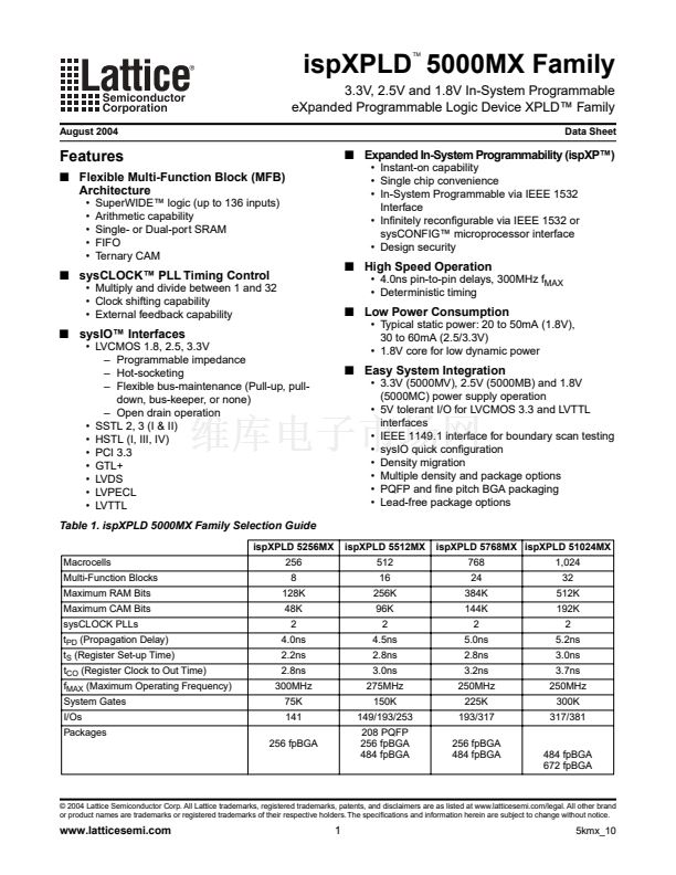
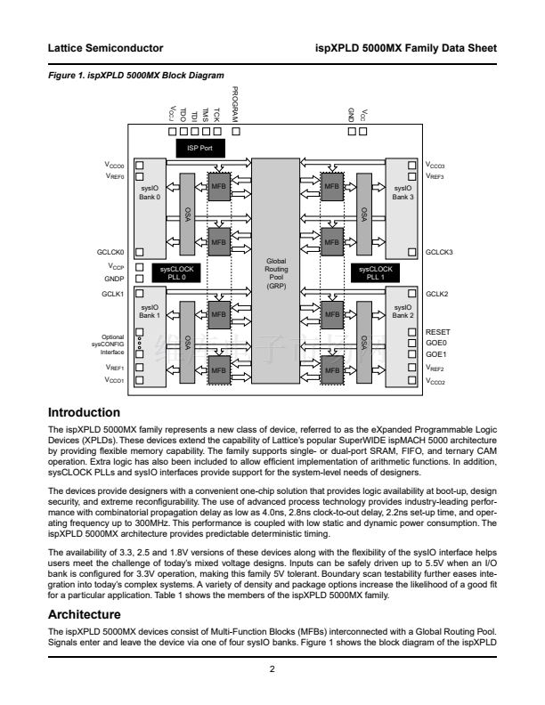
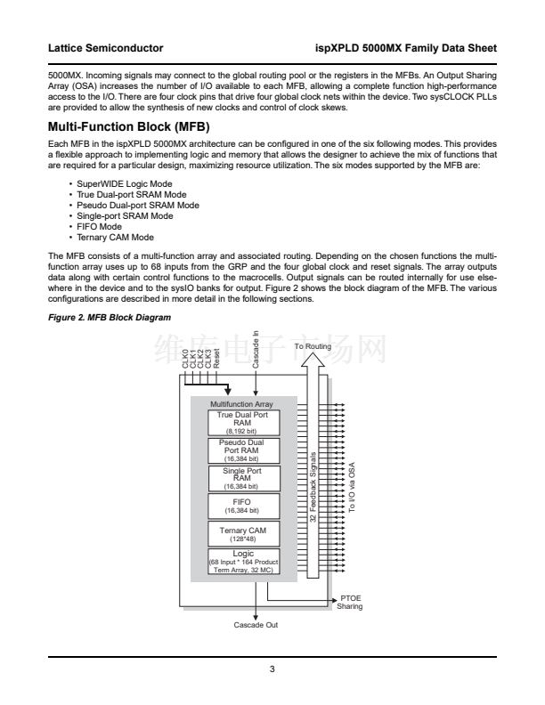
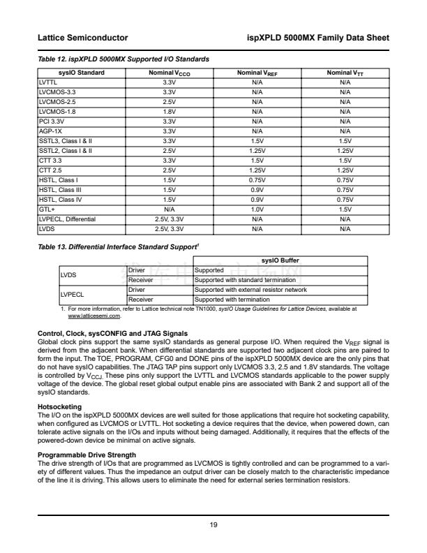
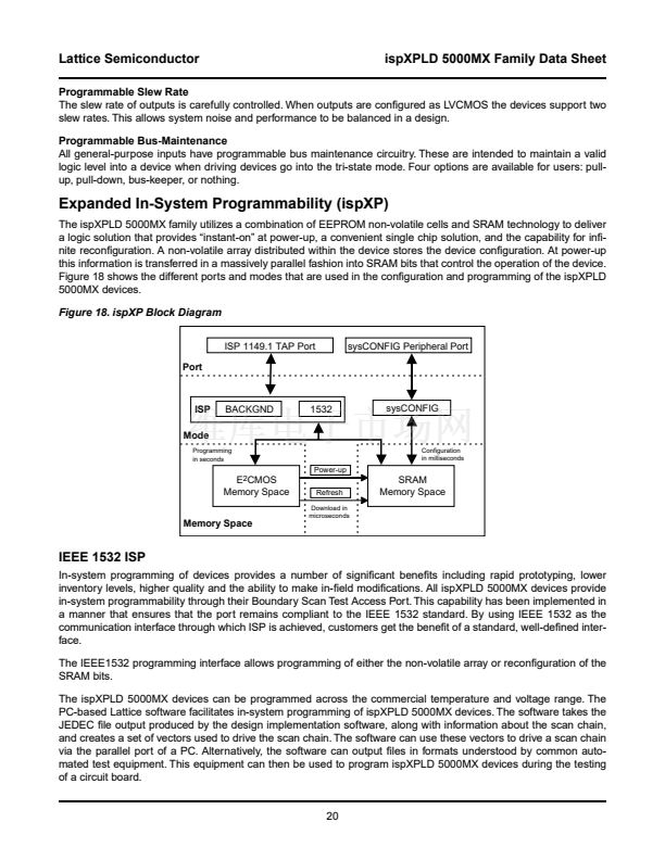
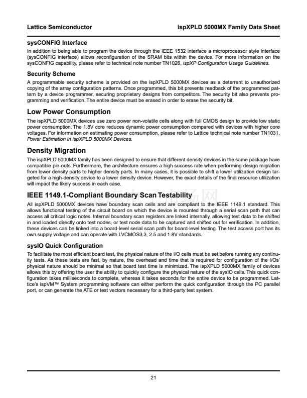
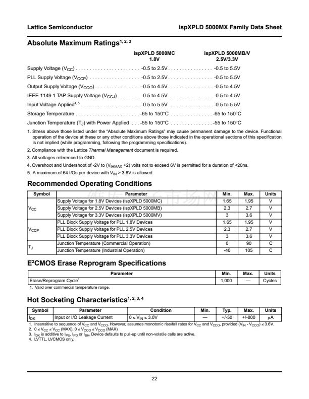
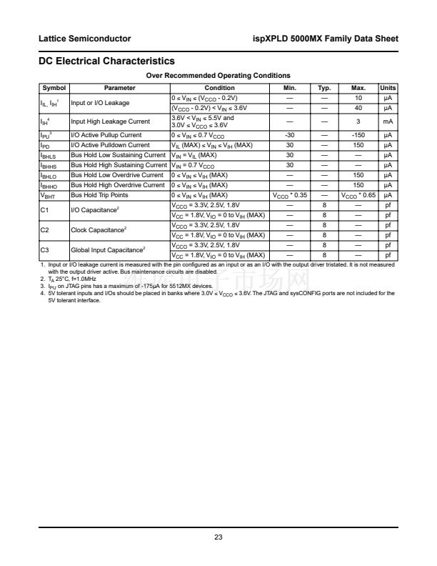
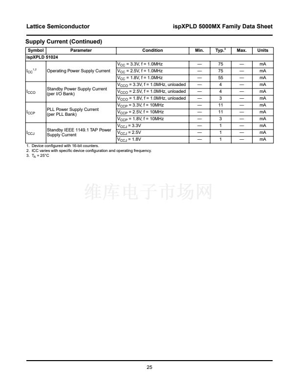
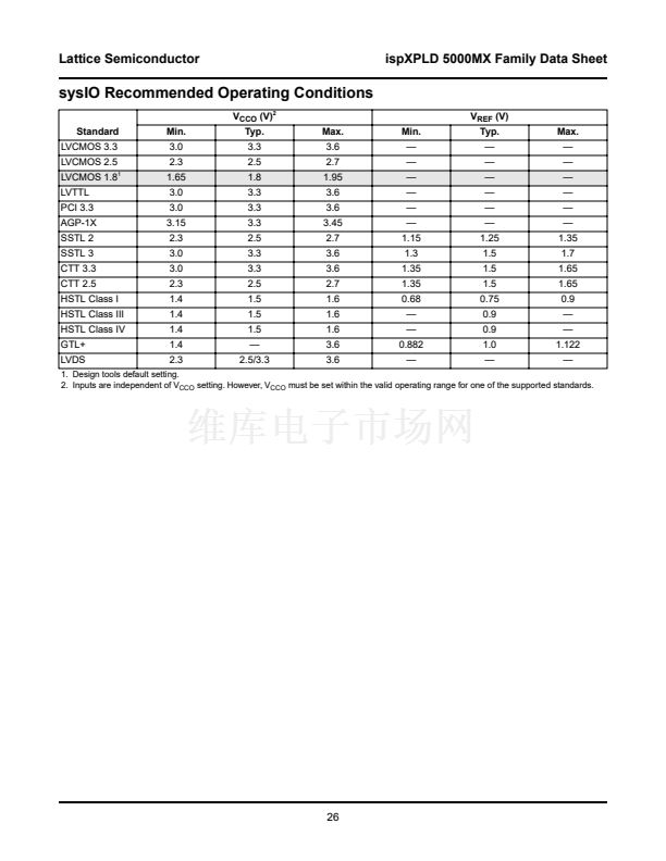
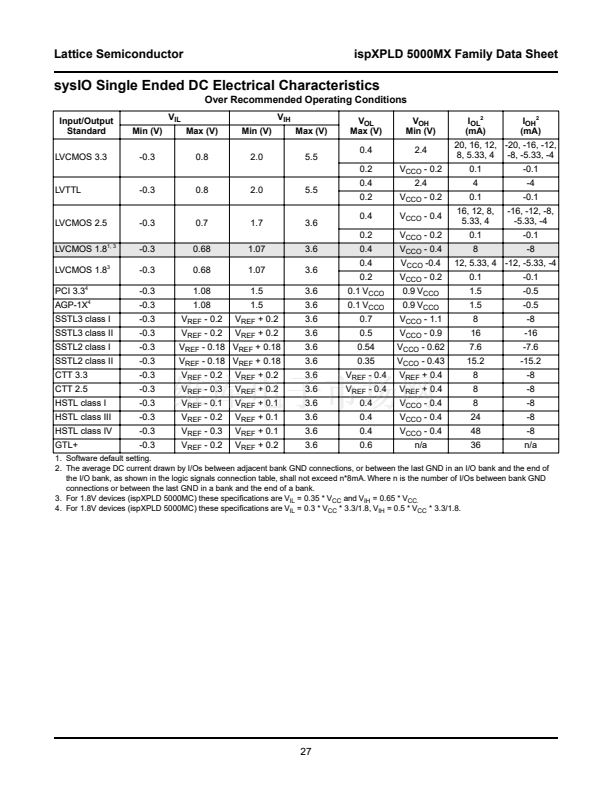
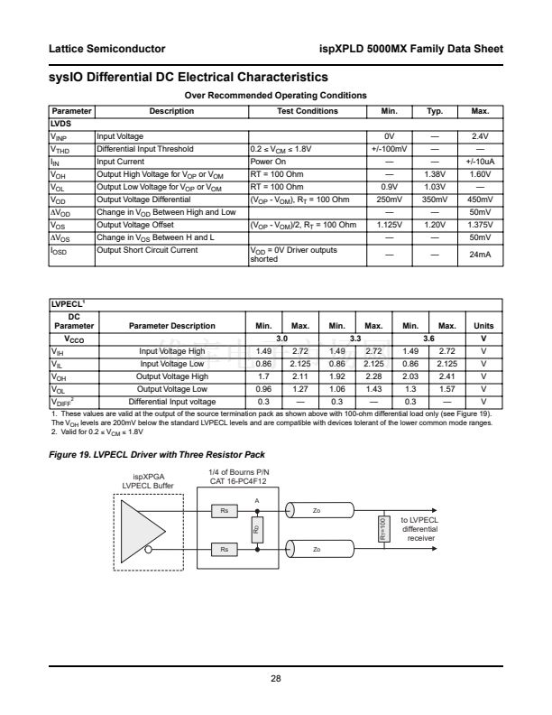
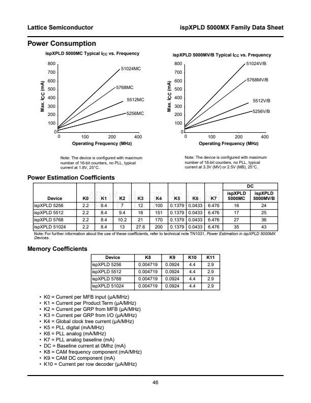
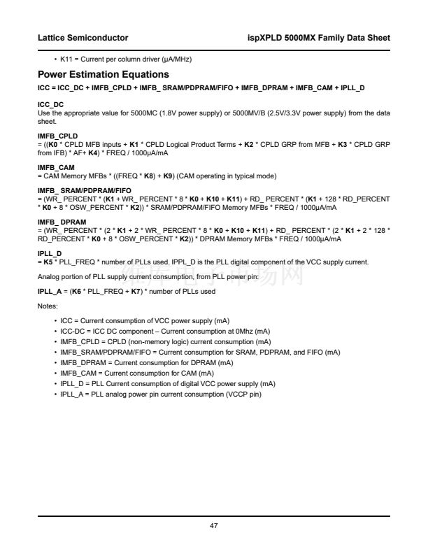
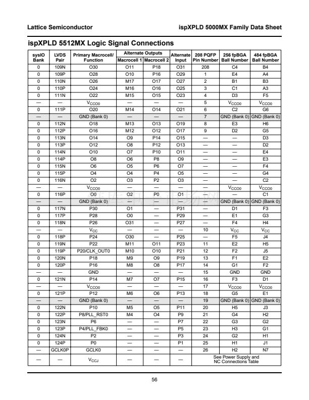
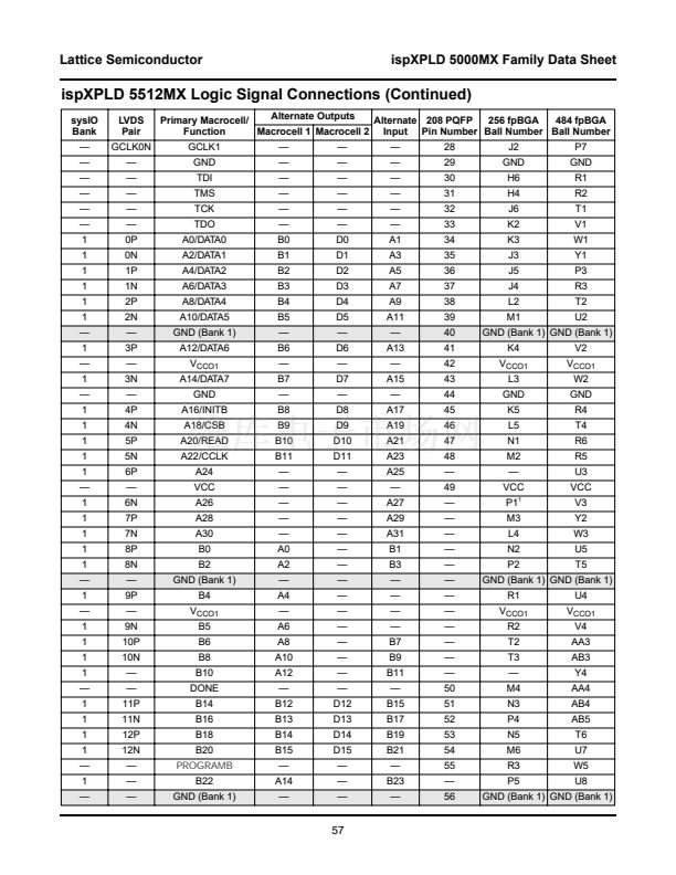
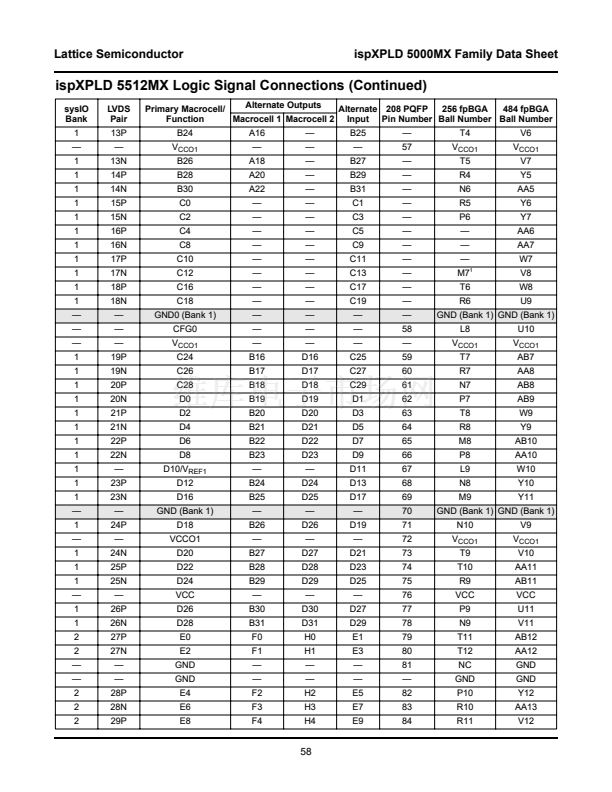
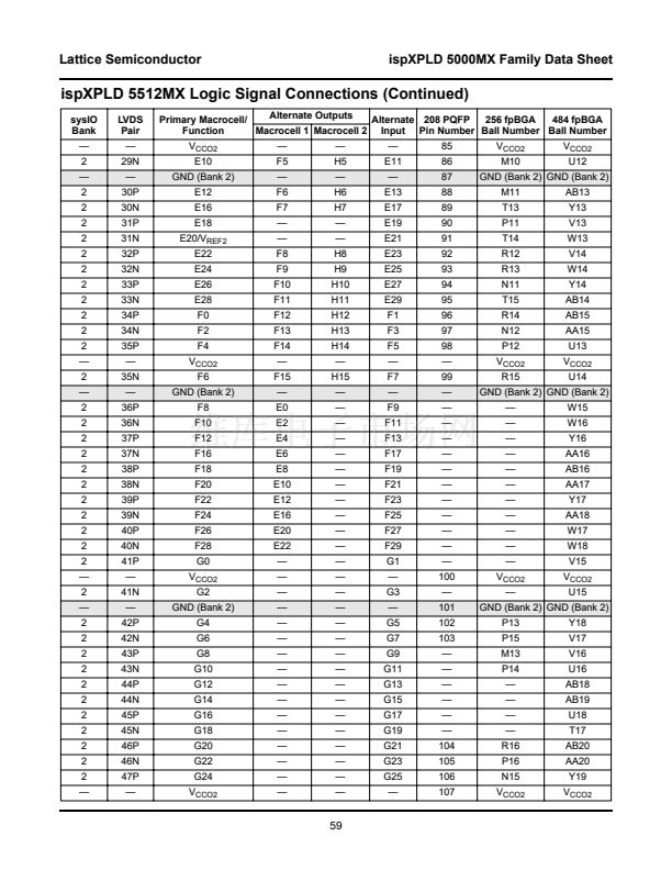
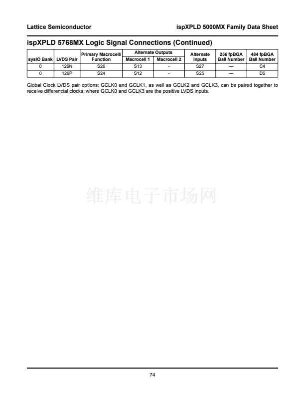
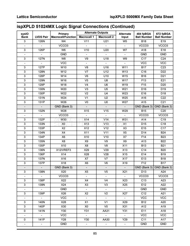
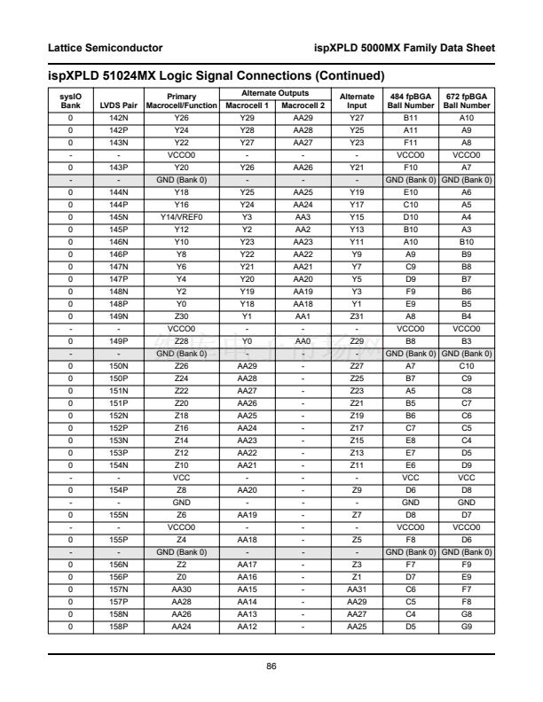
Lattice Semiconductor
ispXPLD 5000MX Family Data Sheet
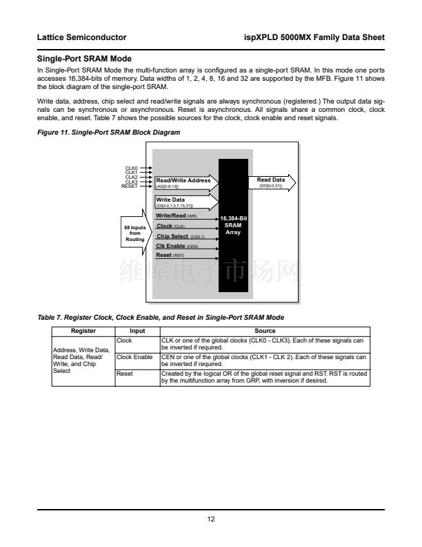
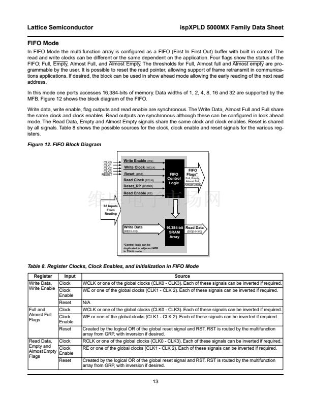
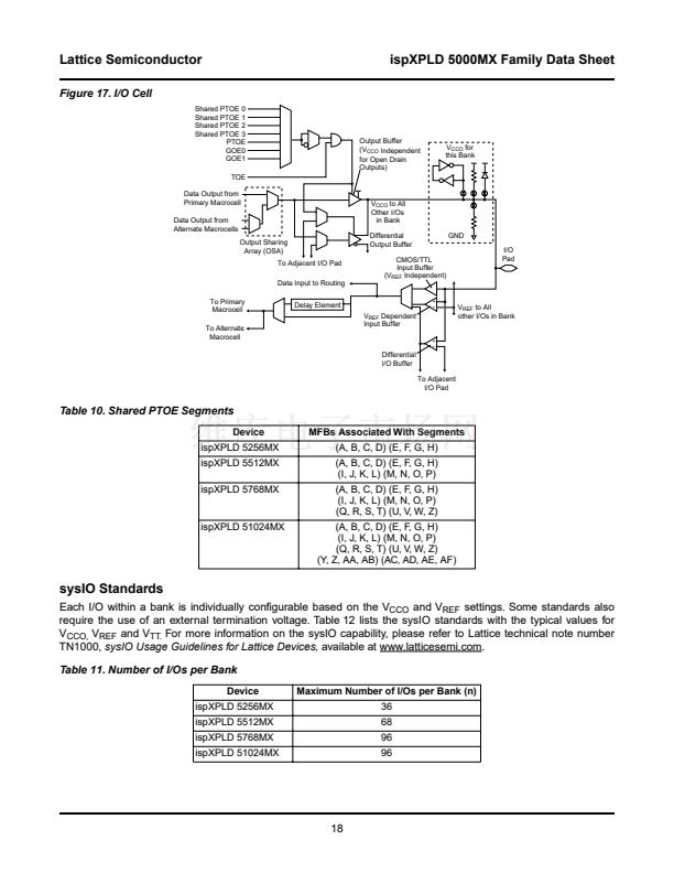
Clock Distribution
The ispXPLD 5000MX family has four dedicated clock input pins: GCLK0-GCLK3. GLCK0 and GCLK3 can be
routed through a PLL circuit or routed directly to the internal clock nets. The internal clock nets (CLK0-CLK3) are
directly related to the dedicated clock pins (see Secondary Clock Divider exception when using the sysCLOCK cir-
cuit). These feed the registers in the MFBs. Note at each register there is the option of inverting the clock if
required. Figure 14 shows the clock distribution network.
Figure 14. Clock Distribution Network
I/O/CLK_OUT0
GCLK0
VREF0
PLL0
SEC_OUT0
CLK_OUT0
CLK0
Clock Net
To Macrocells
CLK1
GCLK1
VREF1
sysCLOCK PLLs
VREF2
GCLK2
CLK2
SEC_OUT1
PLL1
VREF3
GCLK3
CLK_OUT1
CLK3
Clock Net
To Macrocells
Global Clock Routing
Clock Net
To Macrocells
Clock Net
To Macrocells
I/O/CLK_OUT1
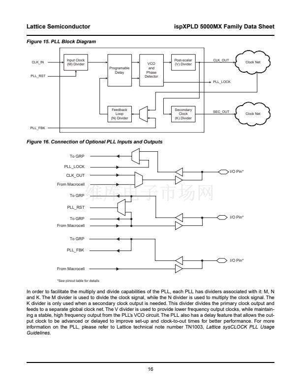
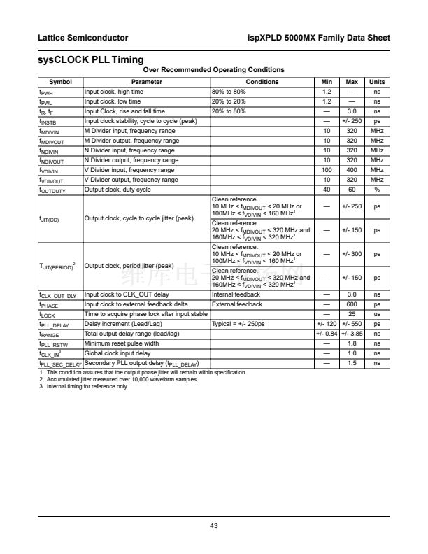
sysCLOCK PLL
The sysCLOCK PLL circuitry consists of Phase-Lock Loops (PLLs) and the various dividers, reset and feedback
signals associated with the PLLs. This feature gives the user the ability to synthesize clock frequencies and gener-
ate multiple clock signals for routing within the device. Furthermore, it can generate clock signals that are de-
skewed either at the board level or the device level.
The ispXPLD 5000MX devices provide two PLL circuits. PLL0 receives its clock inputs from GCLK 0 and provides
outputs to CLK 0 (CLK 1 when using the secondary clock). PLL1 operates with signals from GCLK 3 and CLK 3
(CLK 2 when using the secondary clock). The optional outputs CLK_OUT can be routed to an I/O pin. The optional
PLL_LOCK output is routed into the GRP. The optional input PLL_RST can be routed either from the GRP or
directly from an I/O pin. The optional PLL_FBK into can be routed directly from a pin. Figure 15 shows the ispXPLD
5000MX PLL block diagram. Figure 16 shows the connection of optional inputs and outputs.
15


 1
1
 2
2
 3
3
 4
4
 5
5
 6
6
 7
7
 8
8
 9
9
 10
10
 11
11
 12
12
 13
13
 14
14
 15
15
 16
16
 17
17
 18
18
 19
19
 20
20
 21
21
 22
22
 23
23
 24
24
 25
25
 26
26
 27
27
 28
28
 29
29
 30
30
 31
31
 32
32
 33
33
 34
34
 35
35
 36
36
 37
37
 38
38
 39
39
 40
40
 41
41
 42
42
 43
43
 44
44
 45
45
 46
46
 47
47
 48
48
 49
49
 50
50
 51
51
 52
52
 53
53
 54
54
 55
55
 56
56
 57
57
 58
58
 59
59
 60
60
 61
61
 62
62
 63
63
 64
64
 65
65
 66
66
 67
67
 68
68
 69
69
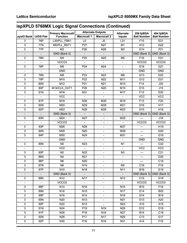
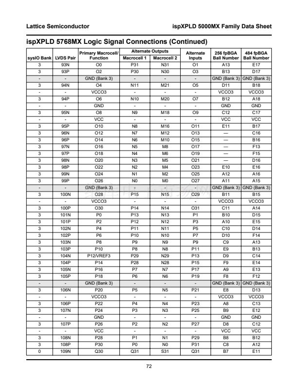
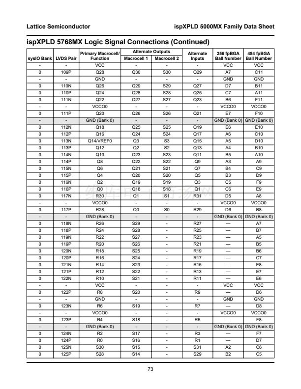
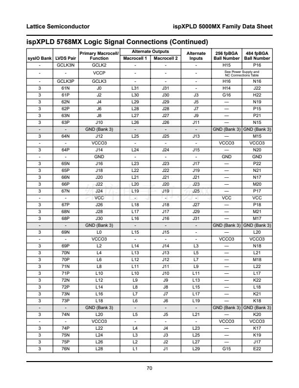 70
70
 71
71
 72
72
 73
73
 74
74
 75
75
 76
76
 77
77
 78
78
 79
79
 80
80
 81
81
 82
82
 83
83
 84
84
 85
85
 86
86
 87
87
 88
88
 89
89
 90
90
 91
91
 92
92
