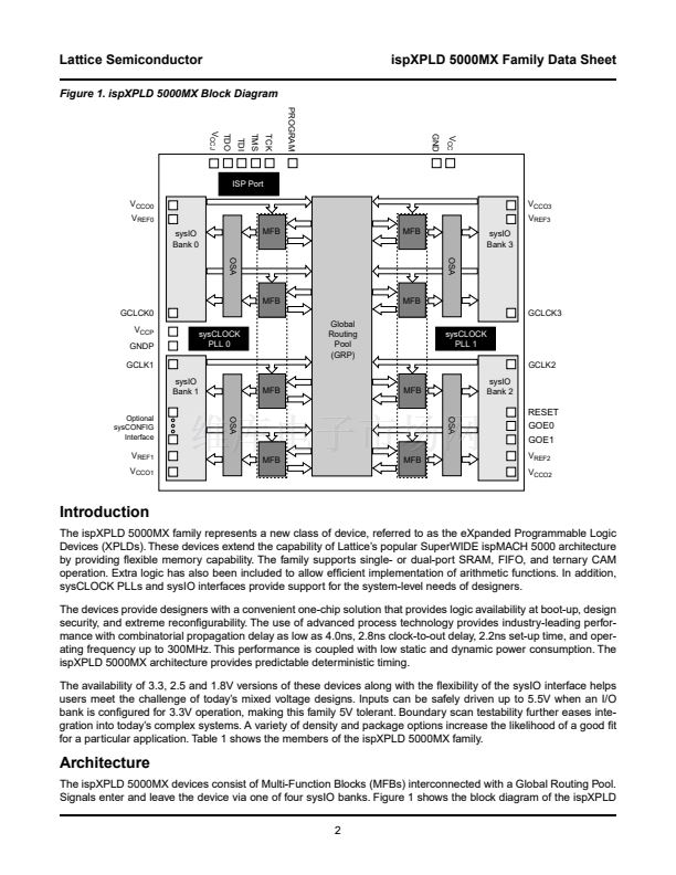
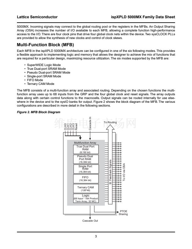
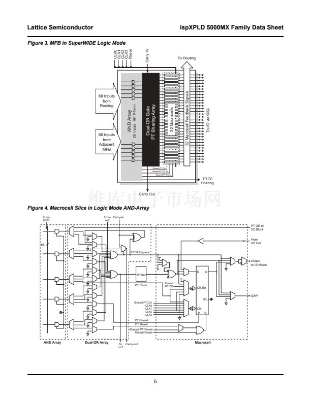
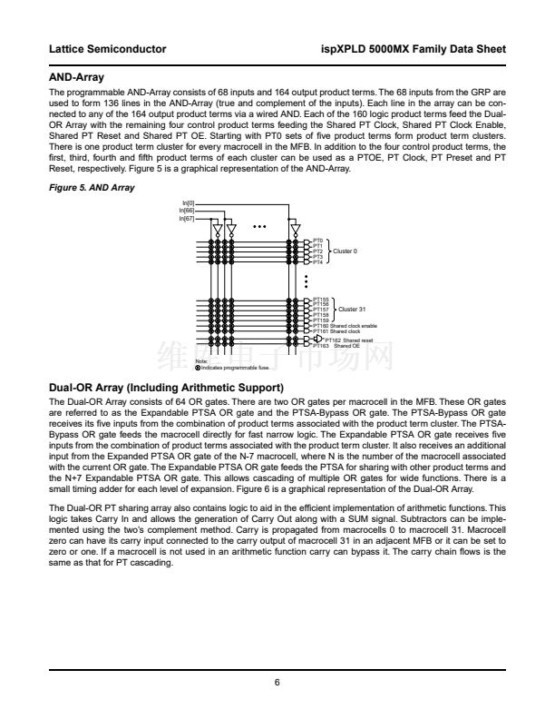
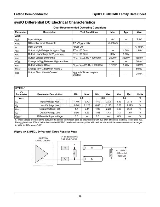
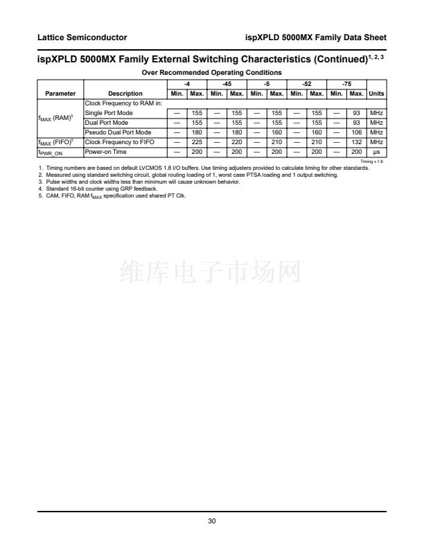
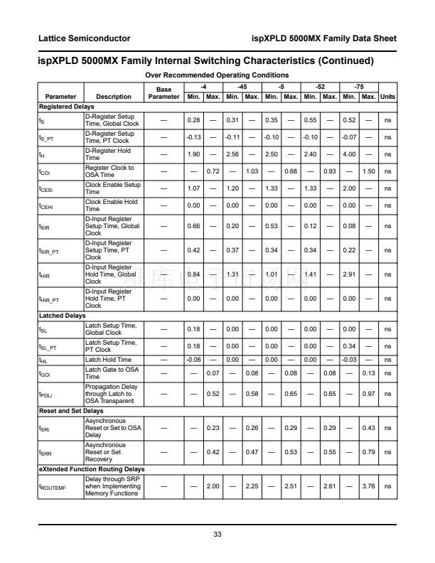
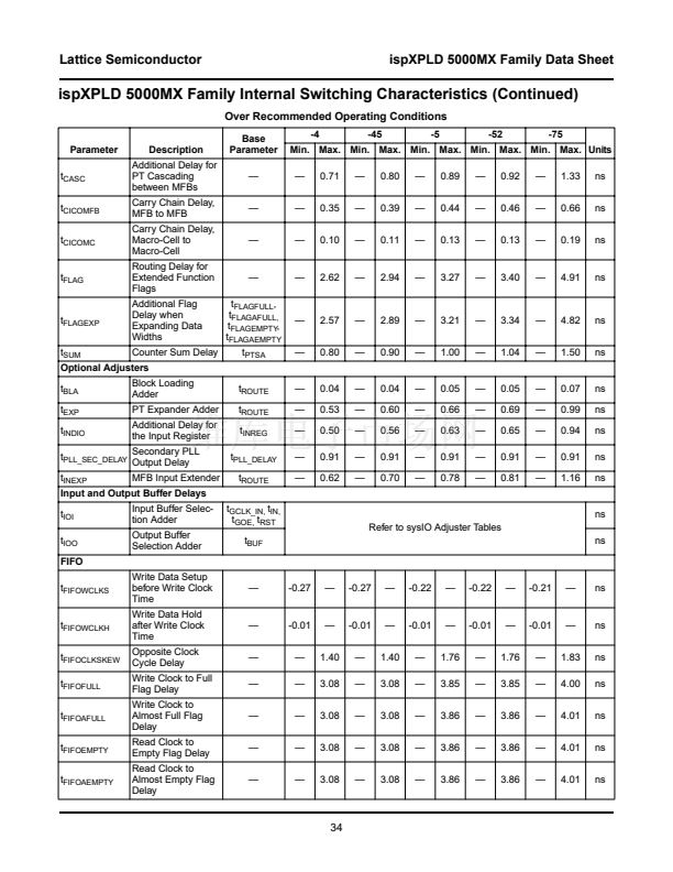
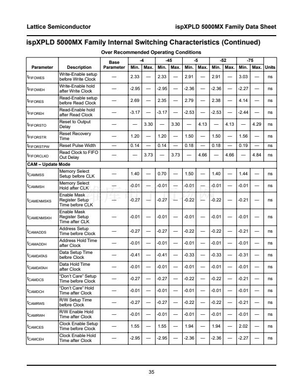
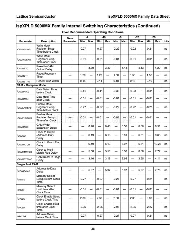
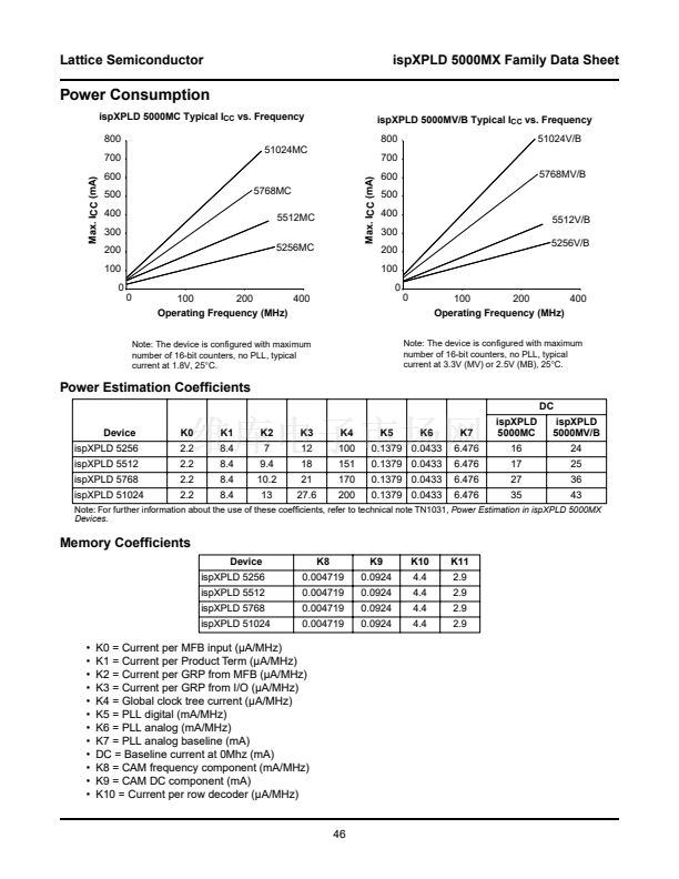
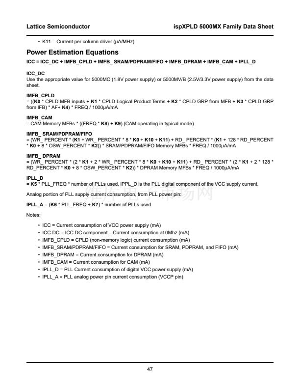
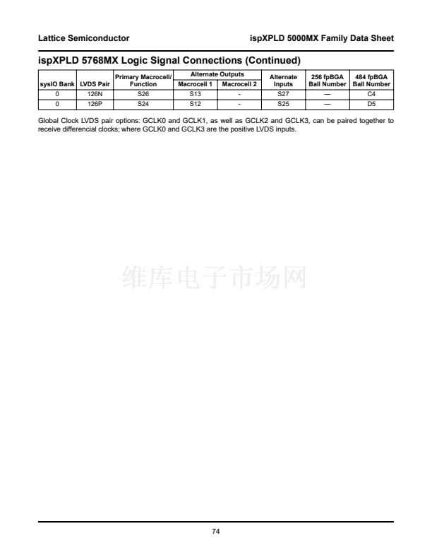
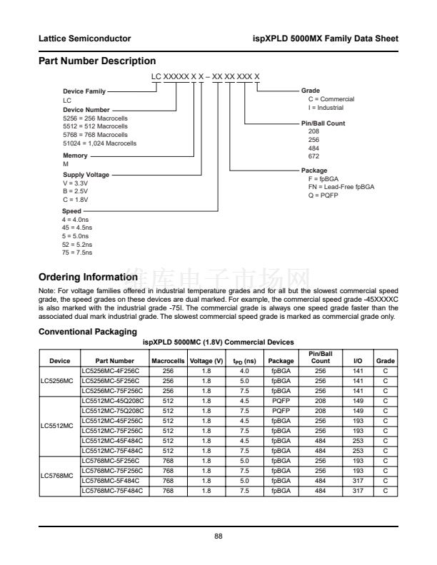
Lattice Semiconductor
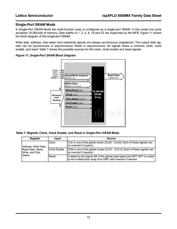
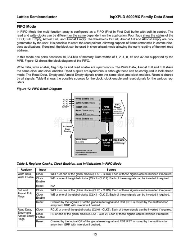
Figure 15. PLL Block Diagram
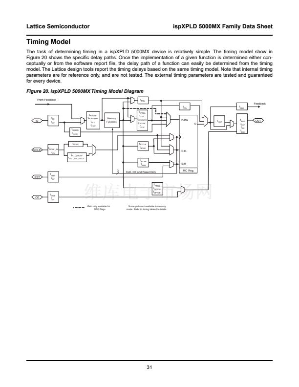
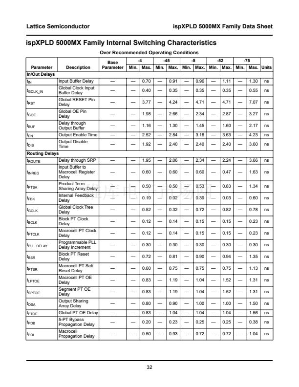
ispXPLD 5000MX Family Data Sheet
CLK_IN
Input Clock
(M) Divider
Programable
Delay
PLL_RST
VCO
and
Phase
Detector
Post-scalar
(V) Divider
CLK_OUT
Clock Net
PLL_LOCK
Feedback
Loop
(N) Divider
PLL_FBK
Secondary
Clock
(K) Divider
SEC_OUT
Clock Net
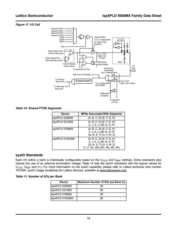
Figure 16. Connection of Optional PLL Inputs and Outputs
To GRP
PLL_LOCK
CLK_OUT
From Macrocell
To GRP
PLL_RST
To GRP
From Macrocell
To GRP
PLL_FBK
I/O Pin*
From Macrocell
*See pinout table for details
I/O Pin*
I/O Pin*
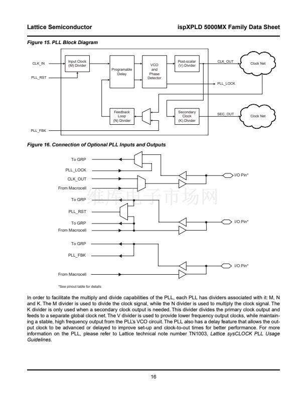
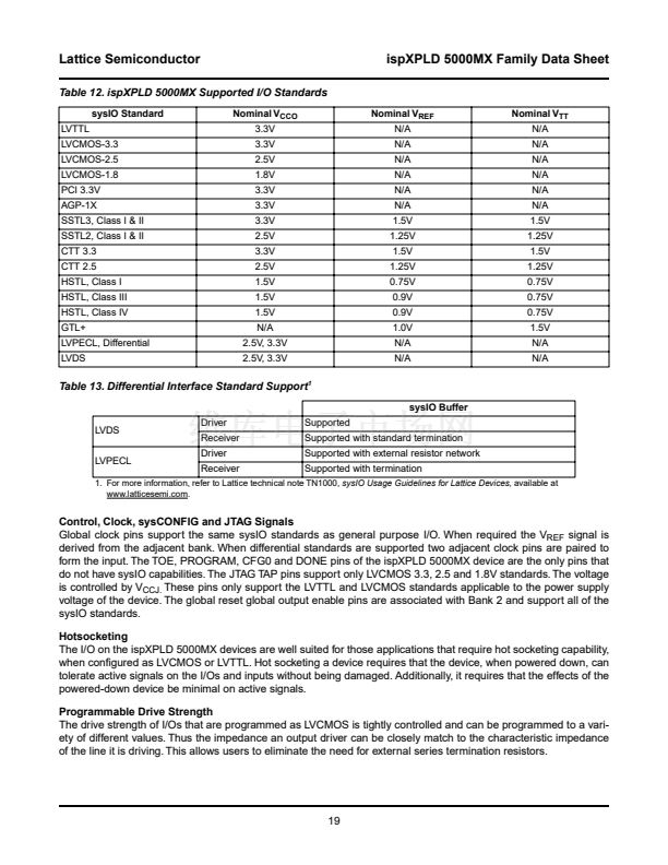
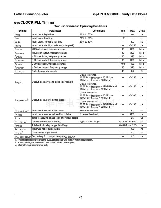
In order to facilitate the multiply and divide capabilities of the PLL, each PLL has dividers associated with it: M, N
and K. The M divider is used to divide the clock signal, while the N divider is used to multiply the clock signal. The
K divider is only used when a secondary clock output is needed. This divider divides the primary clock output and
feeds to a separate global clock net. The V divider is used to provide lower frequency output clocks, while maintain-
ing a stable, high frequency output from the PLL鈥檚 VCO circuit. The PLL also has a delay feature that allows the out-
put clock to be advanced or delayed to improve set-up and clock-to-out times for better performance. For more
information on the PLL, please refer to Lattice technical note number TN1003,
Lattice sysCLOCK PLL Usage
Guidelines.
16


 1
1
 2
2
 3
3
 4
4
 5
5
 6
6
 7
7
 8
8
 9
9
 10
10
 11
11
 12
12
 13
13
 14
14
 15
15
 16
16
 17
17
 18
18
 19
19
 20
20
 21
21
 22
22
 23
23
 24
24
 25
25
 26
26
 27
27
 28
28
 29
29
 30
30
 31
31
 32
32
 33
33
 34
34
 35
35
 36
36
 37
37
 38
38
 39
39
 40
40
 41
41
 42
42
 43
43
 44
44
 45
45
 46
46
 47
47
 48
48
 49
49
 50
50
 51
51
 52
52
 53
53
 54
54
 55
55
 56
56
 57
57
 58
58
 59
59
 60
60
 61
61
 62
62
 63
63
 64
64
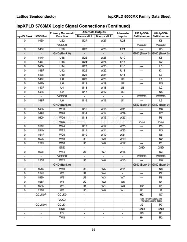 65
65
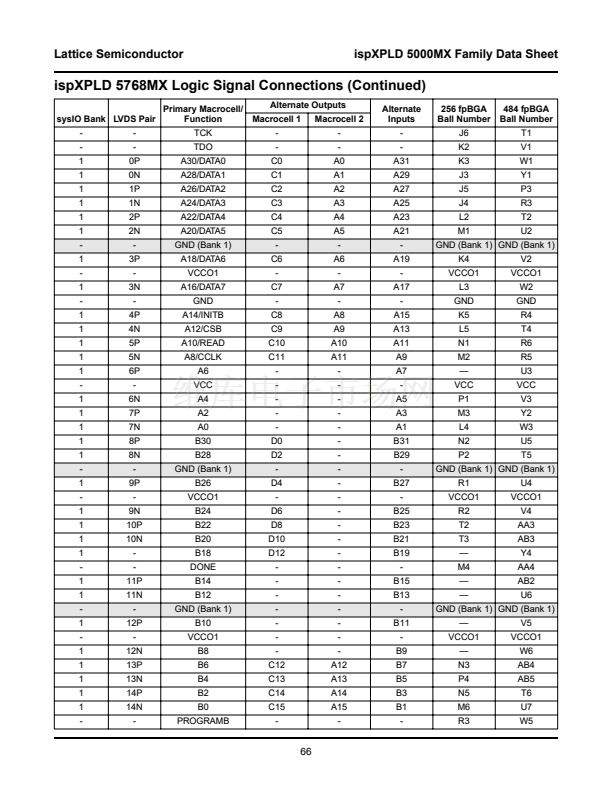 66
66
 67
67
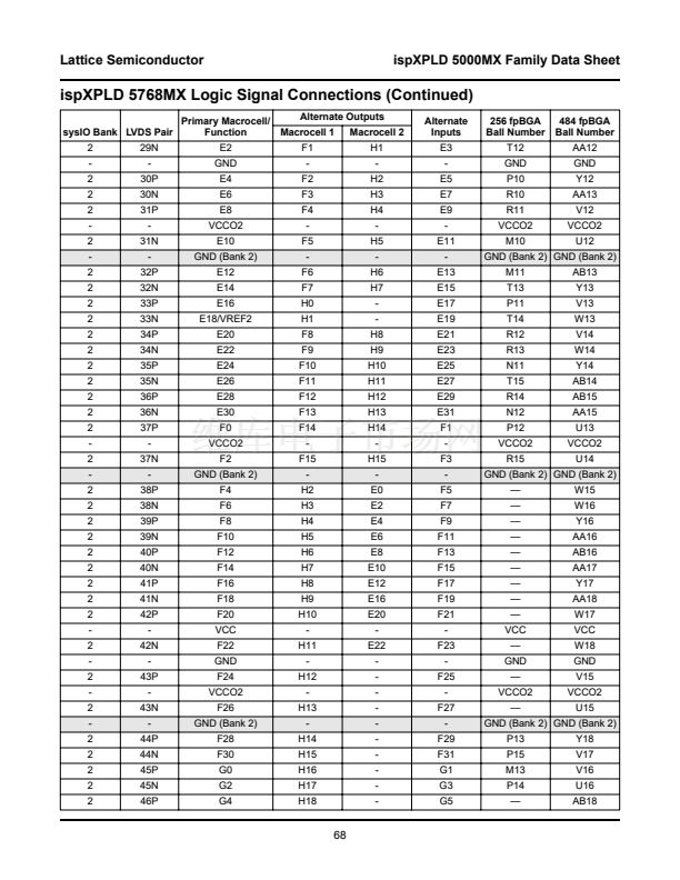 68
68
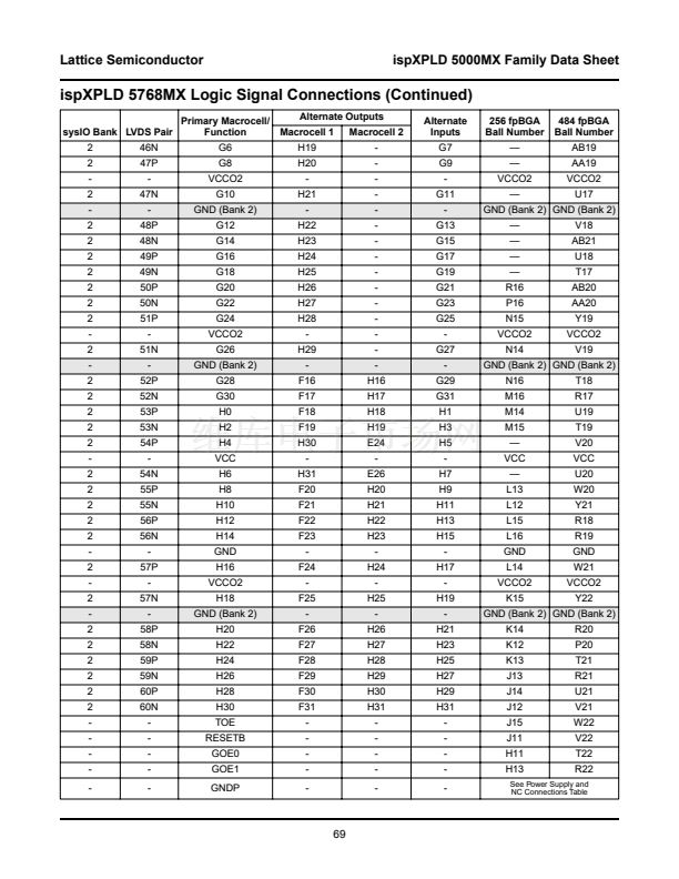 69
69
 70
70
 71
71
 72
72
 73
73
 74
74
 75
75
 76
76
 77
77
 78
78
 79
79
 80
80
 81
81
 82
82
 83
83
 84
84
 85
85
 86
86
 87
87
 88
88
 89
89
 90
90
 91
91
 92
92
