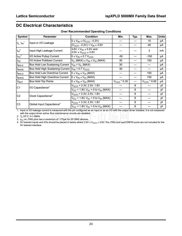
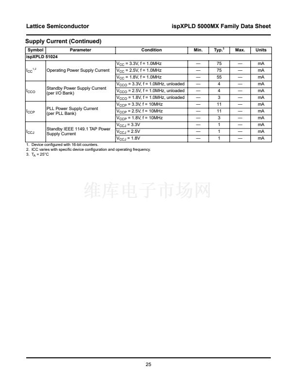
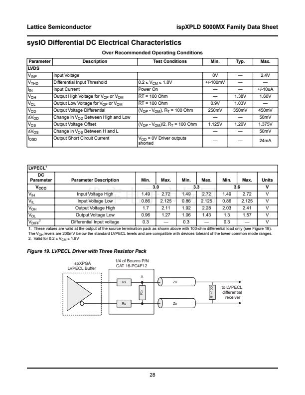
鈥?/div>
V
REF
to All
other I/Os in Bank
Differential
I/O Buffer
To Adjacent
I/O Pad
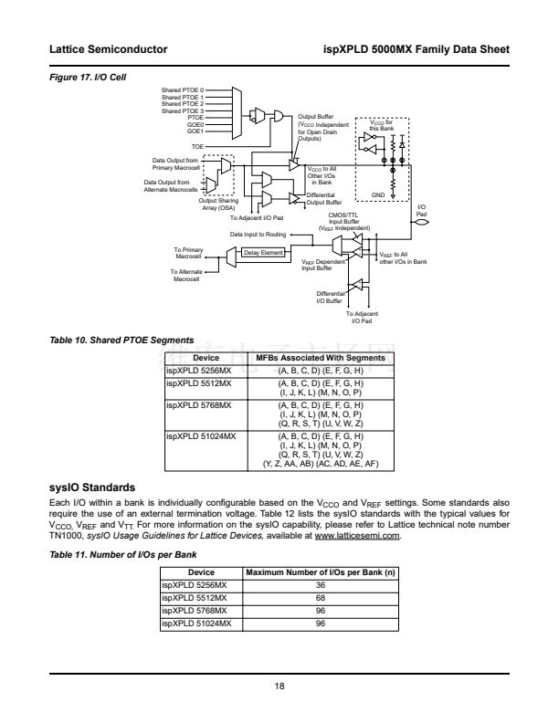
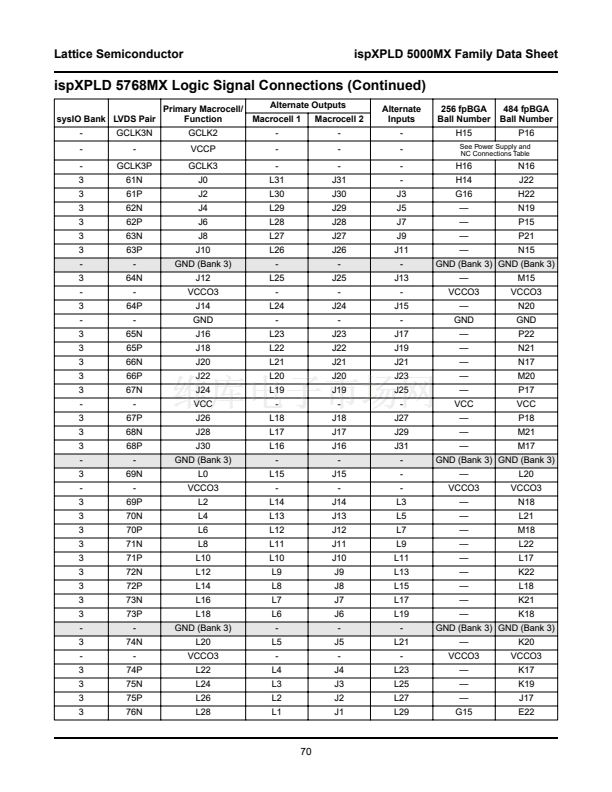
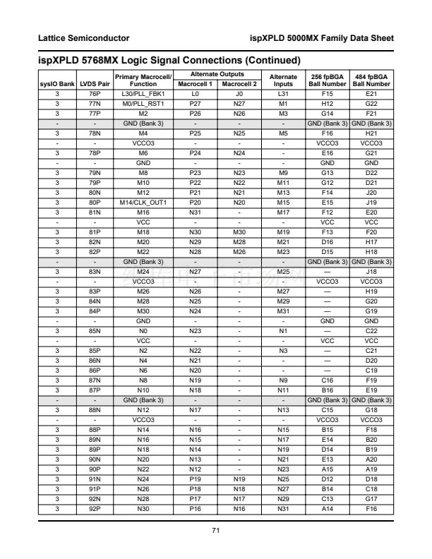
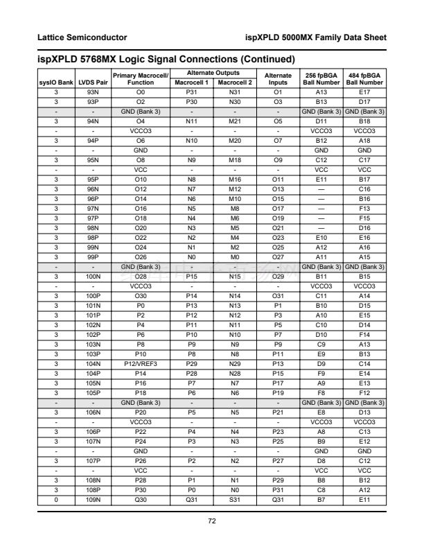
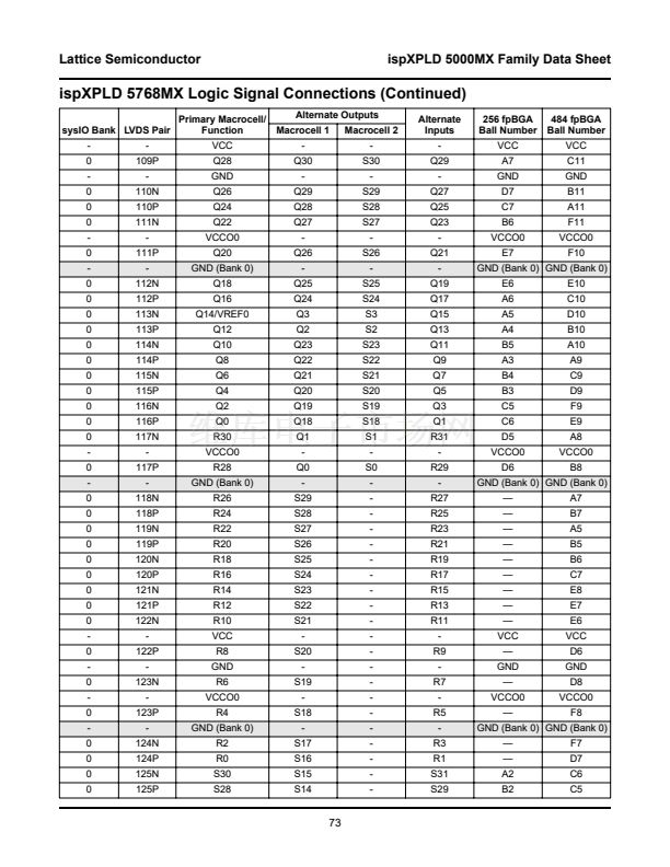
Table 10. Shared PTOE Segments
Device
ispXPLD 5256MX
ispXPLD 5512MX
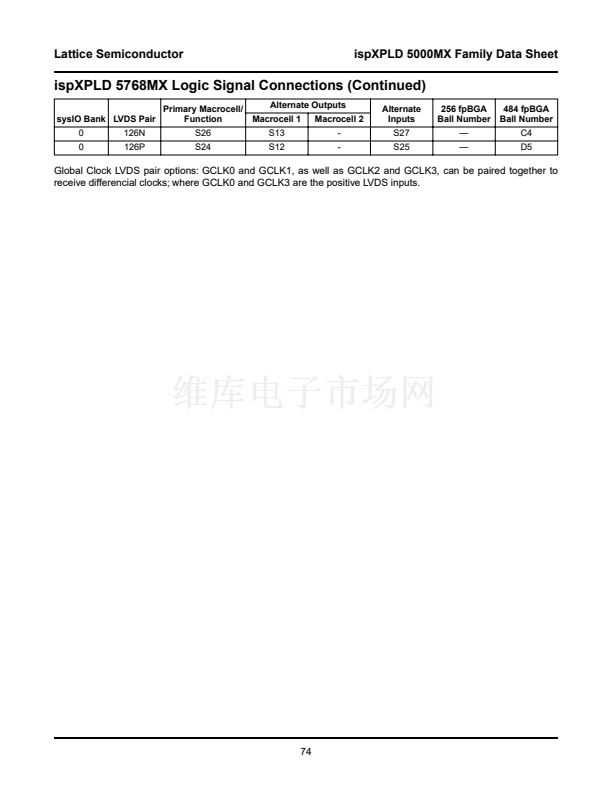
ispXPLD 5768MX
MFBs Associated With Segments
(A, B, C, D) (E, F, G, H)
(A, B, C, D) (E, F, G, H)
(I, J, K, L) (M, N, O, P)
(A, B, C, D) (E, F, G, H)
(I, J, K, L) (M, N, O, P)
(Q, R, S, T) (U, V, W, Z)
(A, B, C, D) (E, F, G, H)
(I, J, K, L) (M, N, O, P)
(Q, R, S, T) (U, V, W, Z)
(Y, Z, AA, AB) (AC, AD, AE, AF)
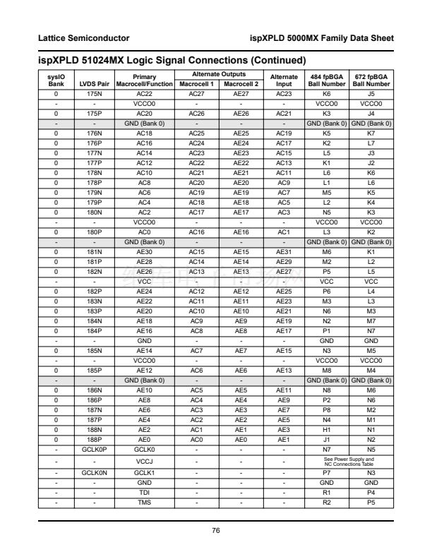
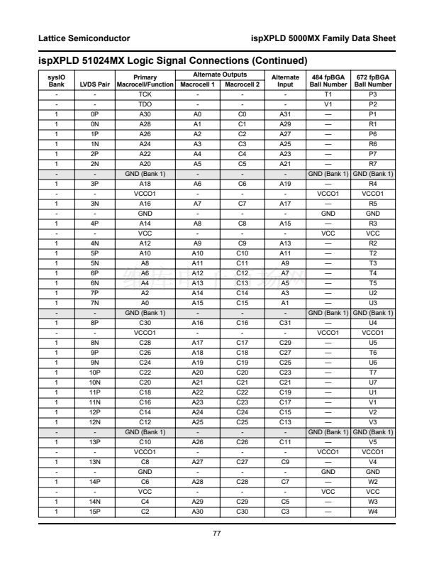
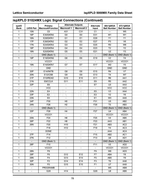
ispXPLD 51024MX
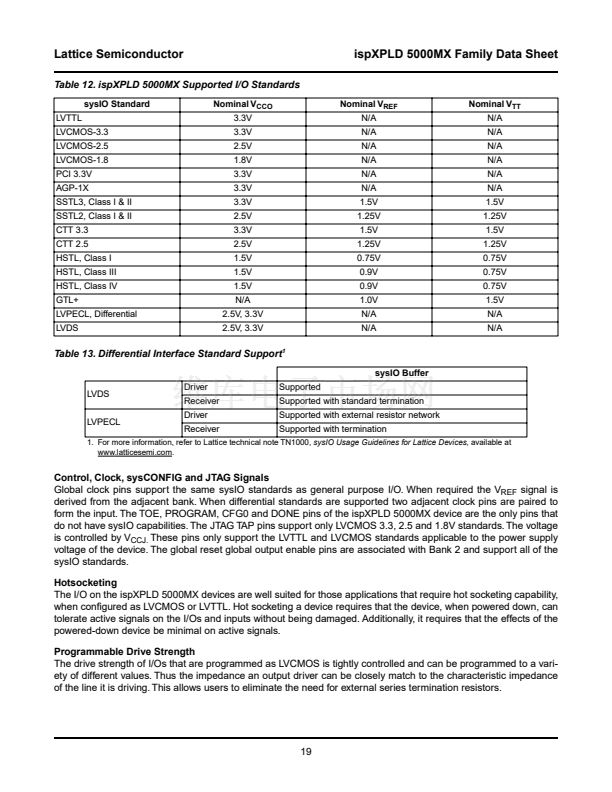
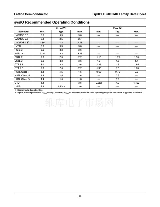
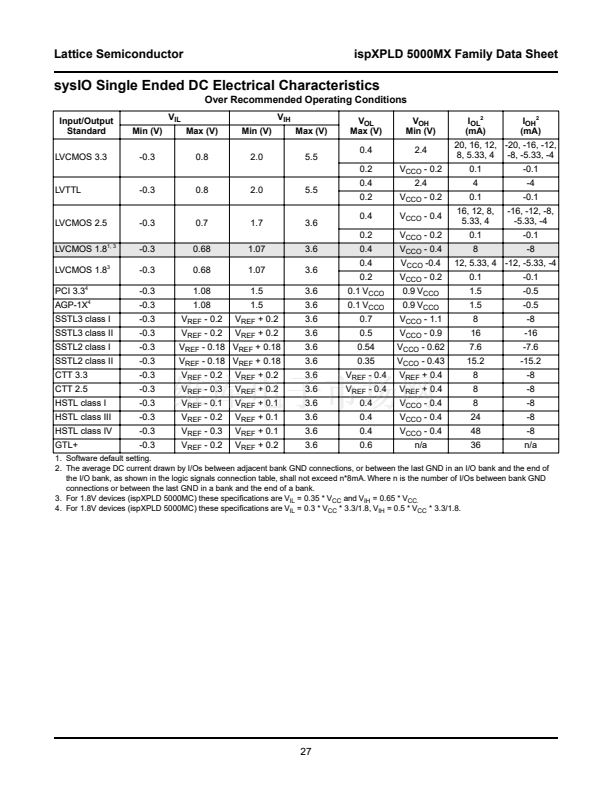
sysIO Standards
Each I/O within a bank is individually con铿乬urable based on the V
CCO
and V
REF
settings. Some standards also
require the use of an external termination voltage. Table 12 lists the sysIO standards with the typical values for
V
CCO,
V
REF
and V
TT.
For more information on the sysIO capability, please refer to Lattice technical note number
TN1000,
sysIO Usage Guidelines for Lattice Devices,
available at www.latticesemi.com.
Table 11. Number of I/Os per Bank
Device
ispXPLD 5256MX
ispXPLD 5512MX
ispXPLD 5768MX
ispXPLD 51024MX
Maximum Number of I/Os per Bank (n)
36
68
96
96
18


 1
1
 2
2
 3
3
 4
4
 5
5
 6
6
 7
7
 8
8
 9
9
 10
10
 11
11
 12
12
 13
13
 14
14
 15
15
 16
16
 17
17
 18
18
 19
19
 20
20
 21
21
 22
22
 23
23
 24
24
 25
25
 26
26
 27
27
 28
28
 29
29
 30
30
 31
31
 32
32
 33
33
 34
34
 35
35
 36
36
 37
37
 38
38
 39
39
 40
40
 41
41
 42
42
 43
43
 44
44
 45
45
 46
46
 47
47
 48
48
 49
49
 50
50
 51
51
 52
52
 53
53
 54
54
 55
55
 56
56
 57
57
 58
58
 59
59
 60
60
 61
61
 62
62
 63
63
 64
64
 65
65
 66
66
 67
67
 68
68
 69
69
 70
70
 71
71
 72
72
 73
73
 74
74
 75
75
 76
76
 77
77
 78
78
 79
79
 80
80
 81
81
 82
82
 83
83
 84
84
 85
85
 86
86
 87
87
 88
88
 89
89
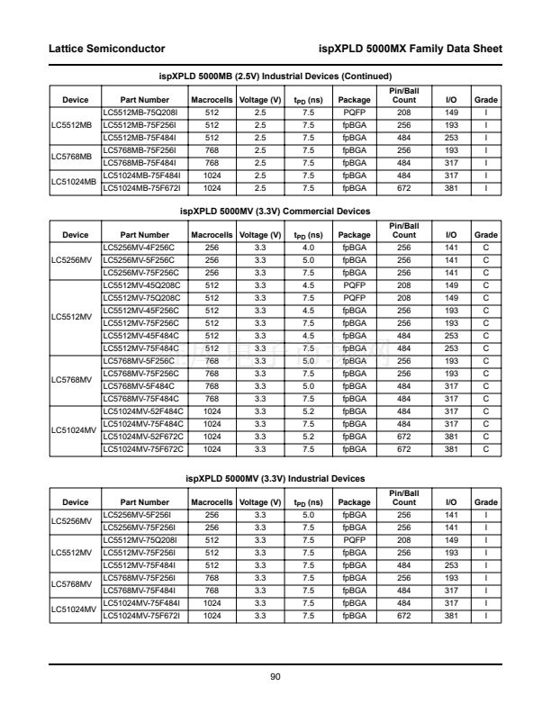 90
90
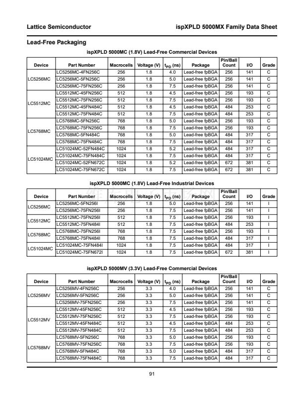 91
91
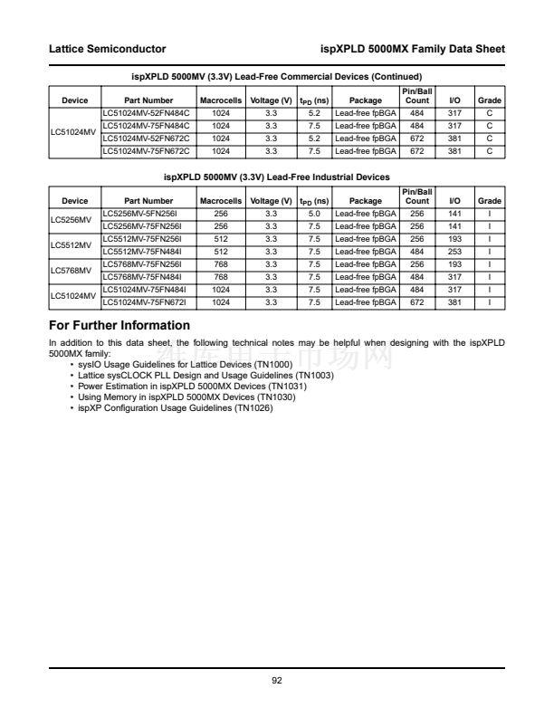 92
92
