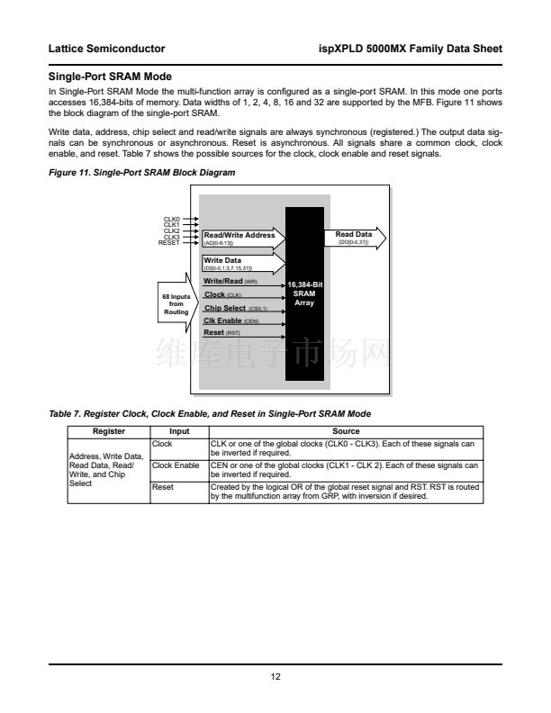
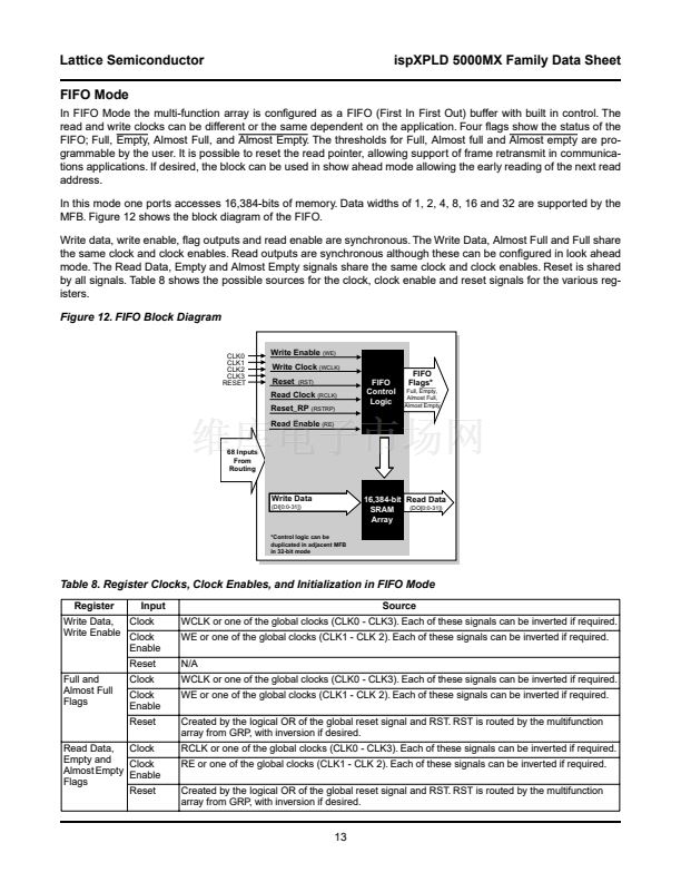
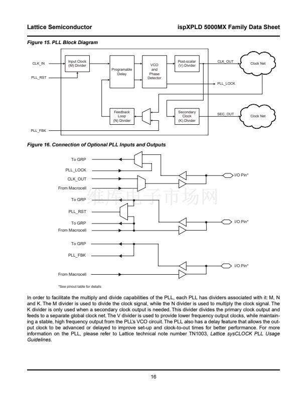
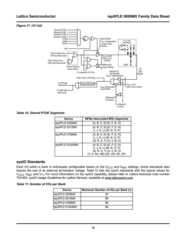
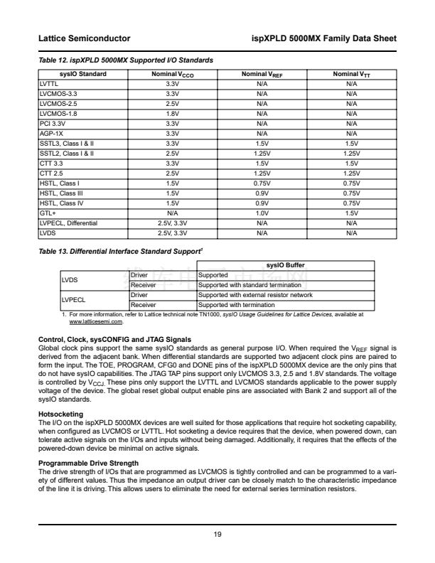
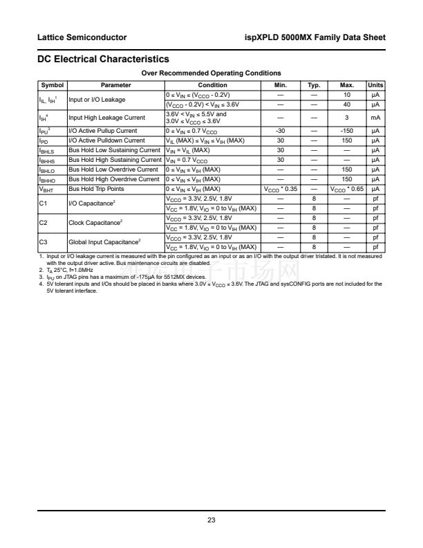
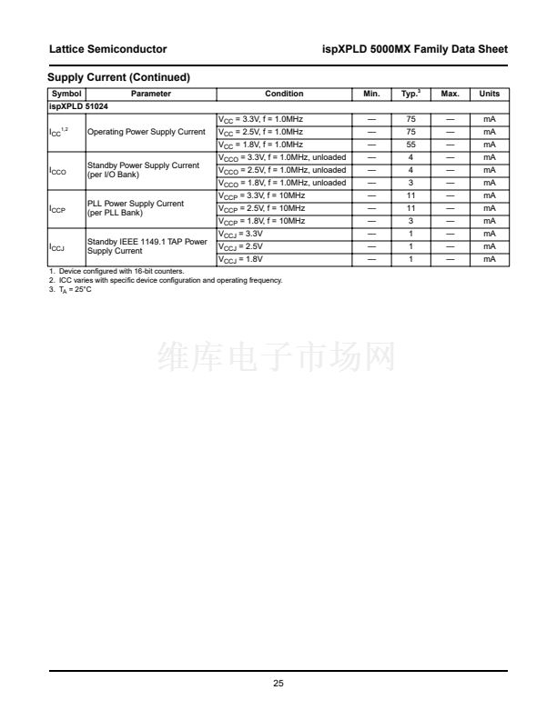
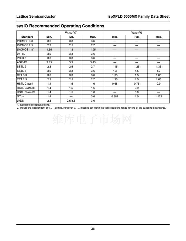
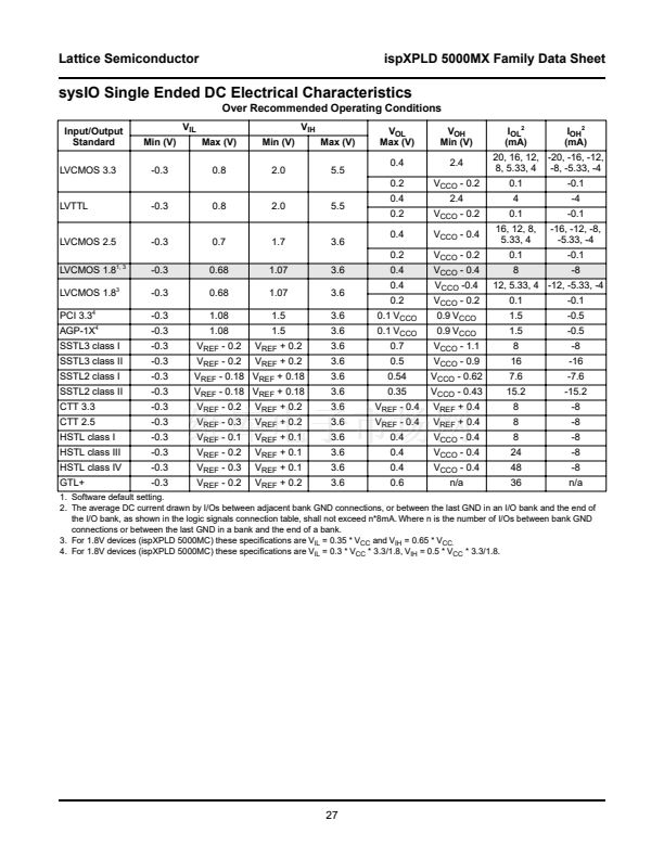
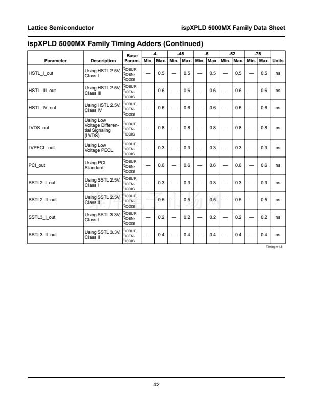
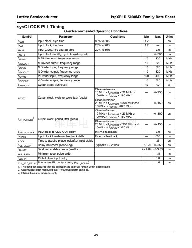
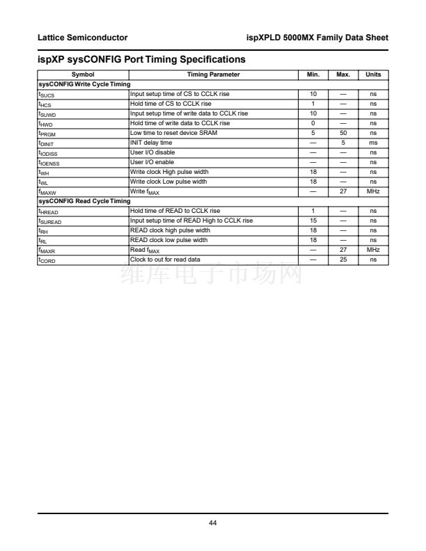
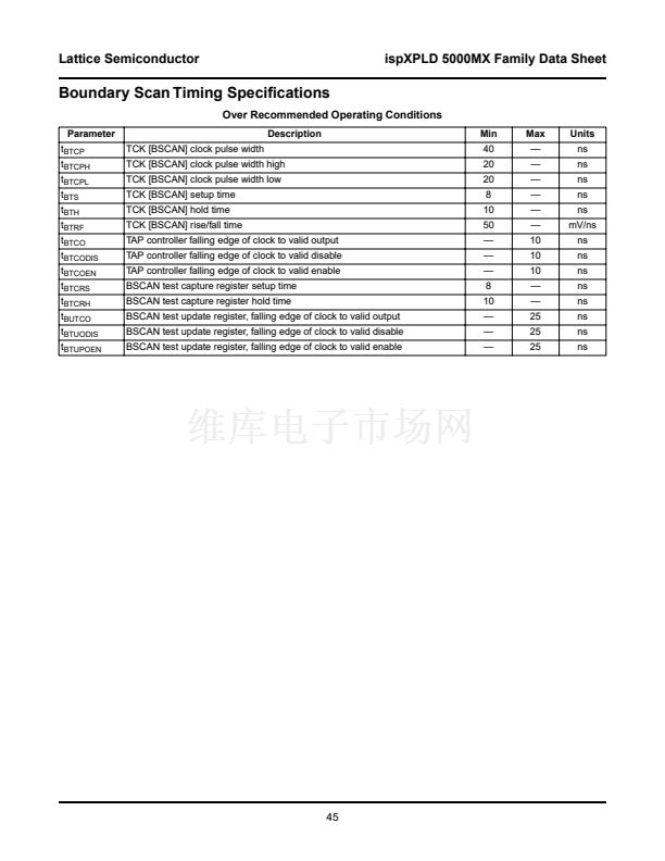
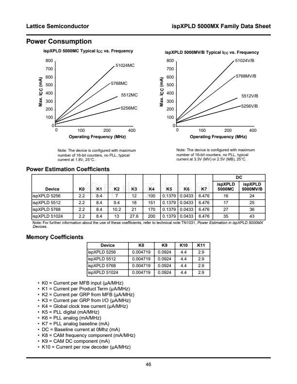
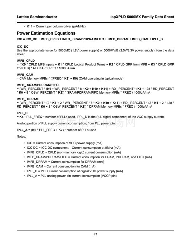
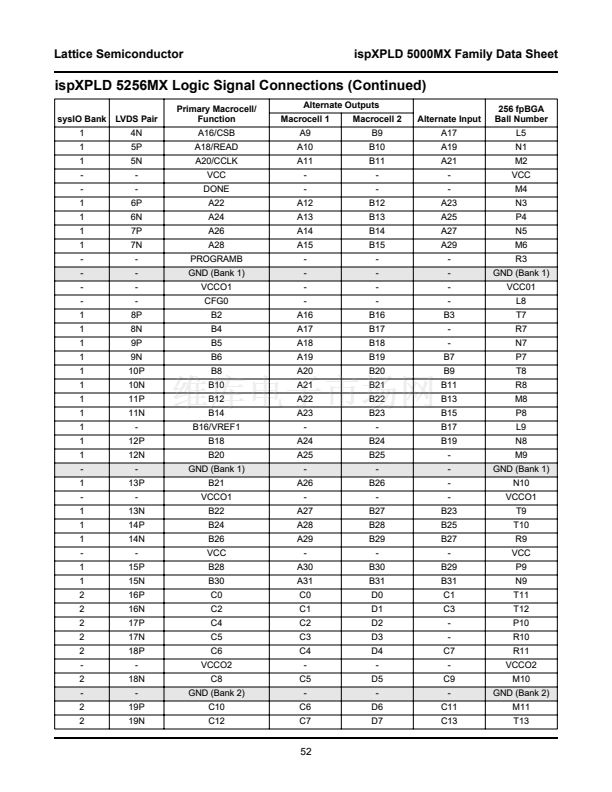
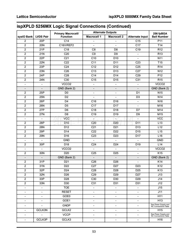
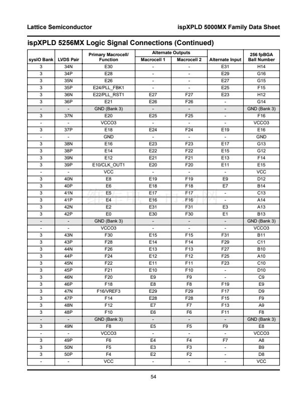
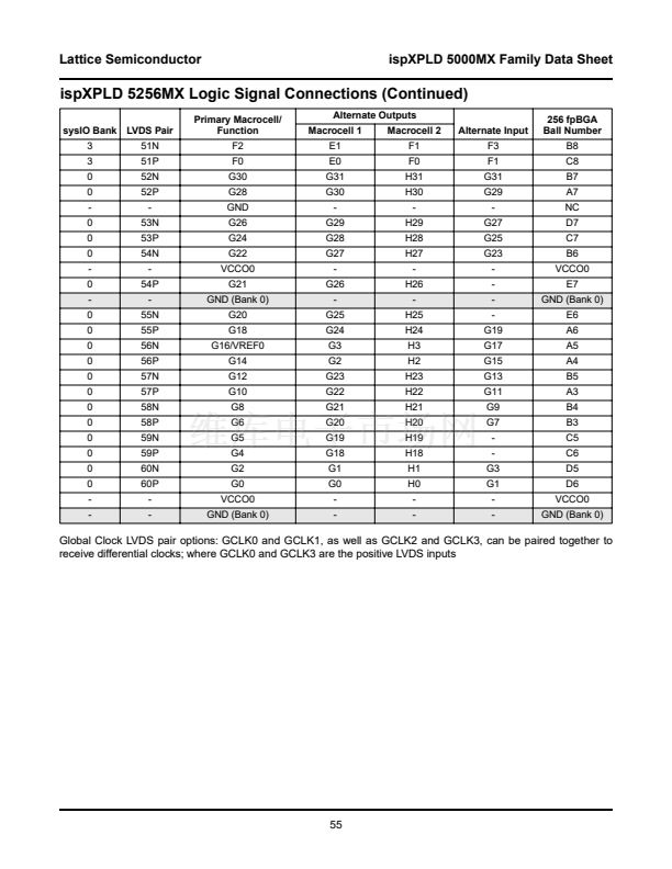
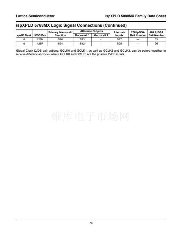
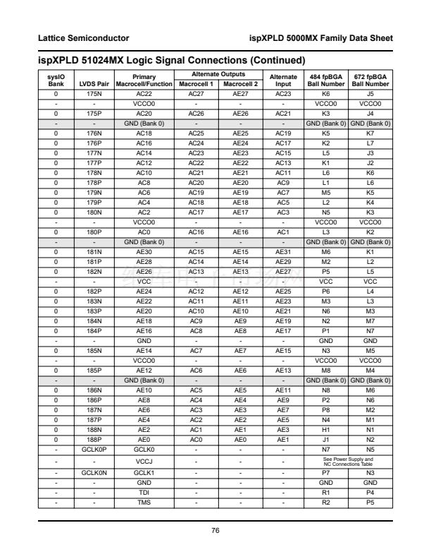
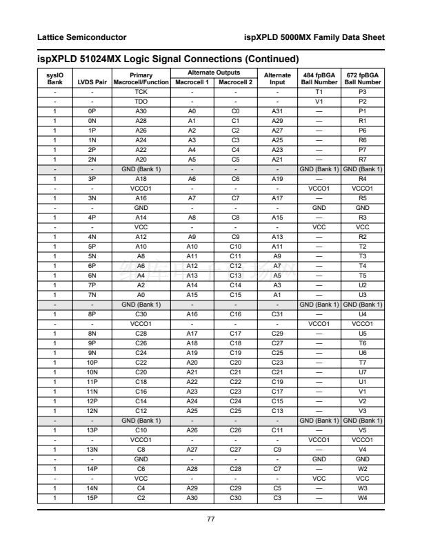
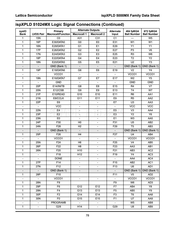
Lattice Semiconductor
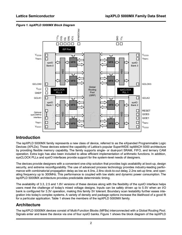
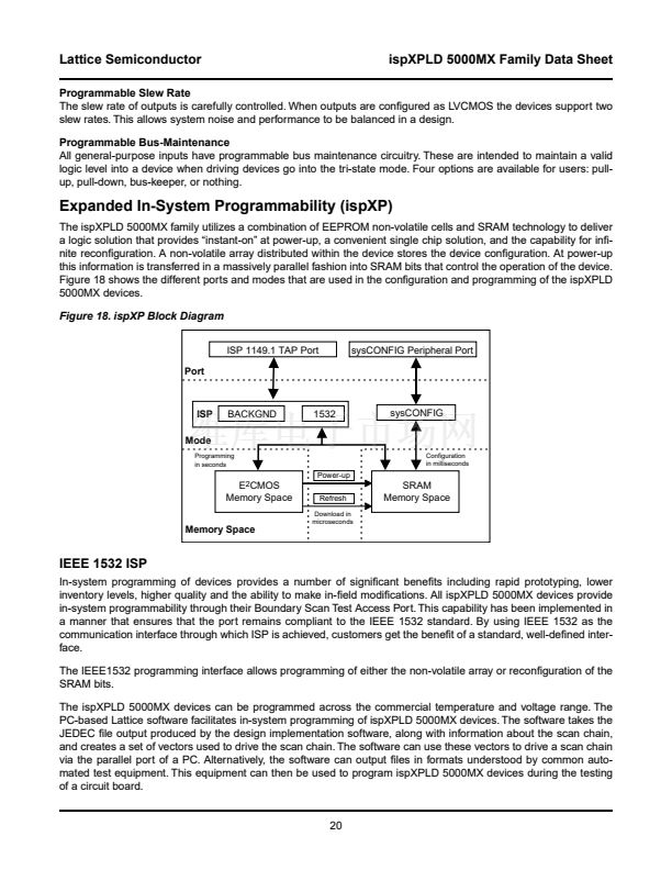
Figure 1. ispXPLD 5000MX Block Diagram
PROGRAM
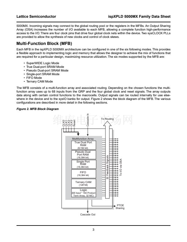
ispXPLD 5000MX Family Data Sheet
TDO
V
CCJ
GND
TMS
TCK
V
CC
ISP Port
V
CCO0
V
REF0
sysIO
Bank 0
OSA
TDI
V
CCO3
V
REF3
MFB
MFB
sysIO
Bank 3
OSA
MFB
GCLCK0
V
CCP
GNDP
GCLK1
sysIO
Bank 1
Optional
sysCONFIG
Interface
MFB
GCLCK3
Global
Routing
Pool
(GRP)
sysCLOCK
PLL 0
sysCLOCK
PLL 1
GCLK2
MFB
MFB
sysIO
Bank 2
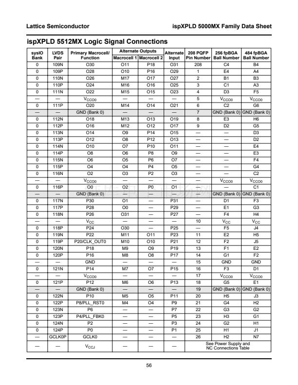
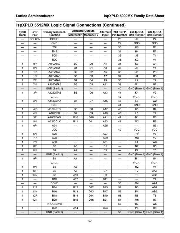
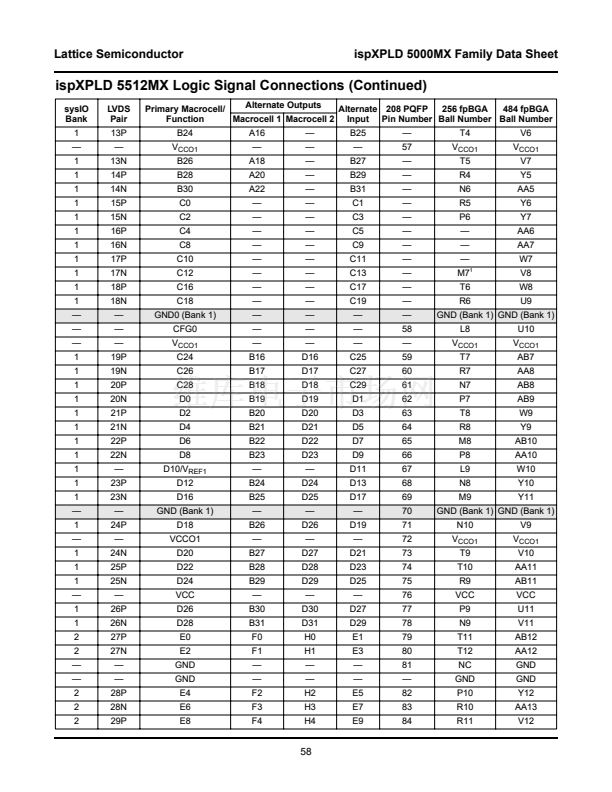
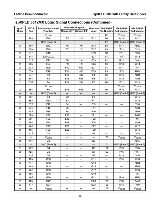
RESET
GOE0
GOE1
V
REF2
V
CCO2
OSA
OSA
V
REF1
V
CCO1
MFB
MFB
Introduction
The ispXPLD 5000MX family represents a new class of device, referred to as the eXpanded Programmable Logic
Devices (XPLDs). These devices extend the capability of Lattice鈥檚 popular SuperWIDE ispMACH 5000 architecture
by providing 铿俥xible memory capability. The family supports single- or dual-port SRAM, FIFO, and ternary CAM
operation. Extra logic has also been included to allow ef铿乧ient implementation of arithmetic functions. In addition,
sysCLOCK PLLs and sysIO interfaces provide support for the system-level needs of designers.
The devices provide designers with a convenient one-chip solution that provides logic availability at boot-up, design
security, and extreme recon铿乬urability. The use of advanced process technology provides industry-leading perfor-
mance with combinatorial propagation delay as low as 4.0ns, 2.8ns clock-to-out delay, 2.2ns set-up time, and oper-
ating frequency up to 300MHz. This performance is coupled with low static and dynamic power consumption. The
ispXPLD 5000MX architecture provides predictable deterministic timing.
The availability of 3.3, 2.5 and 1.8V versions of these devices along with the 铿俥xibility of the sysIO interface helps
users meet the challenge of today鈥檚 mixed voltage designs. Inputs can be safely driven up to 5.5V when an I/O
bank is con铿乬ured for 3.3V operation, making this family 5V tolerant. Boundary scan testability further eases inte-
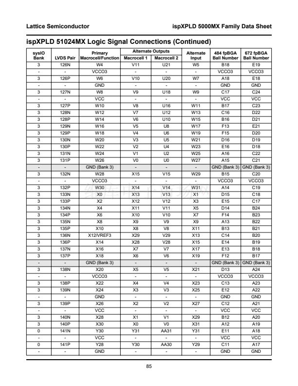
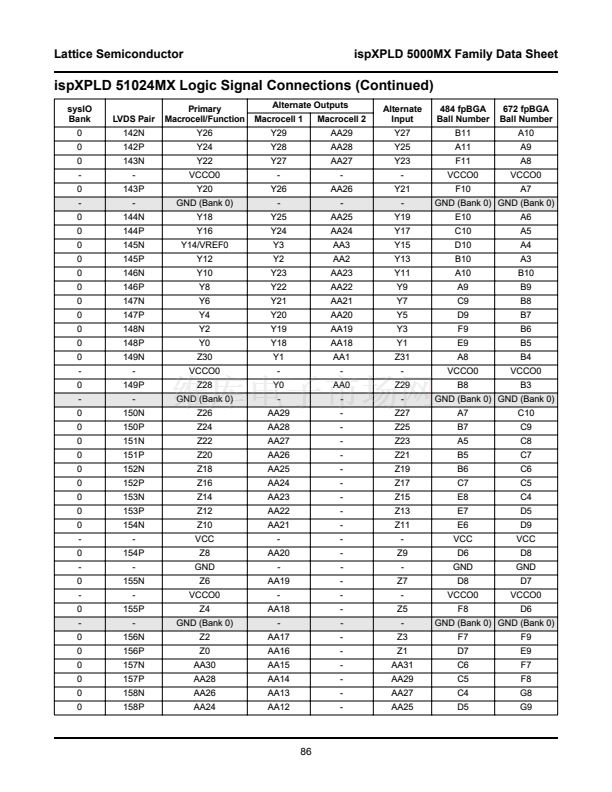
gration into today鈥檚 complex systems. A variety of density and package options increase the likelihood of a good 铿乼
for a particular application. Table 1 shows the members of the ispXPLD 5000MX family.
Architecture
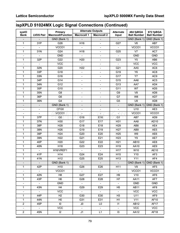
The ispXPLD 5000MX devices consist of Multi-Function Blocks (MFBs) interconnected with a Global Routing Pool.
Signals enter and leave the device via one of four sysIO banks. Figure 1 shows the block diagram of the ispXPLD
2


 1
1
 2
2
 3
3
 4
4
 5
5
 6
6
 7
7
 8
8
 9
9
 10
10
 11
11
 12
12
 13
13
 14
14
 15
15
 16
16
 17
17
 18
18
 19
19
 20
20
 21
21
 22
22
 23
23
 24
24
 25
25
 26
26
 27
27
 28
28
 29
29
 30
30
 31
31
 32
32
 33
33
 34
34
 35
35
 36
36
 37
37
 38
38
 39
39
 40
40
 41
41
 42
42
 43
43
 44
44
 45
45
 46
46
 47
47
 48
48
 49
49
 50
50
 51
51
 52
52
 53
53
 54
54
 55
55
 56
56
 57
57
 58
58
 59
59
 60
60
 61
61
 62
62
 63
63
 64
64
 65
65
 66
66
 67
67
 68
68
 69
69
 70
70
 71
71
 72
72
 73
73
 74
74
 75
75
 76
76
 77
77
 78
78
 79
79
 80
80
 81
81
 82
82
 83
83
 84
84
 85
85
 86
86
 87
87
 88
88
 89
89
 90
90
 91
91
 92
92
