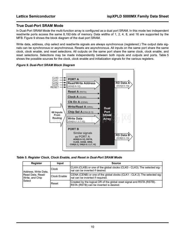
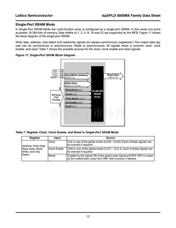
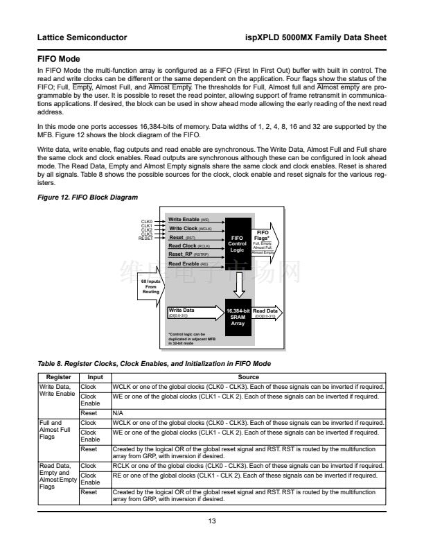
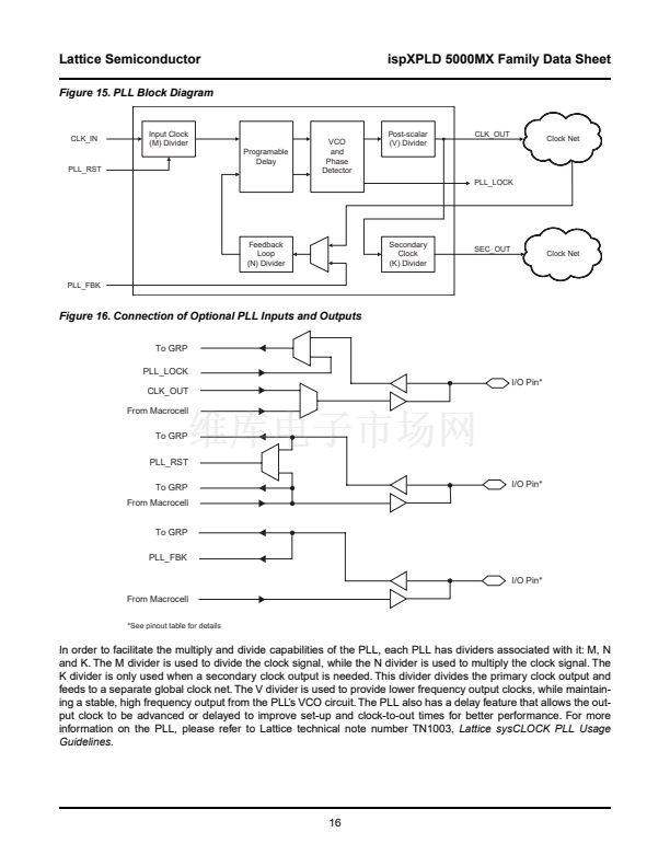
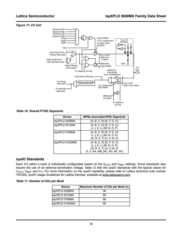
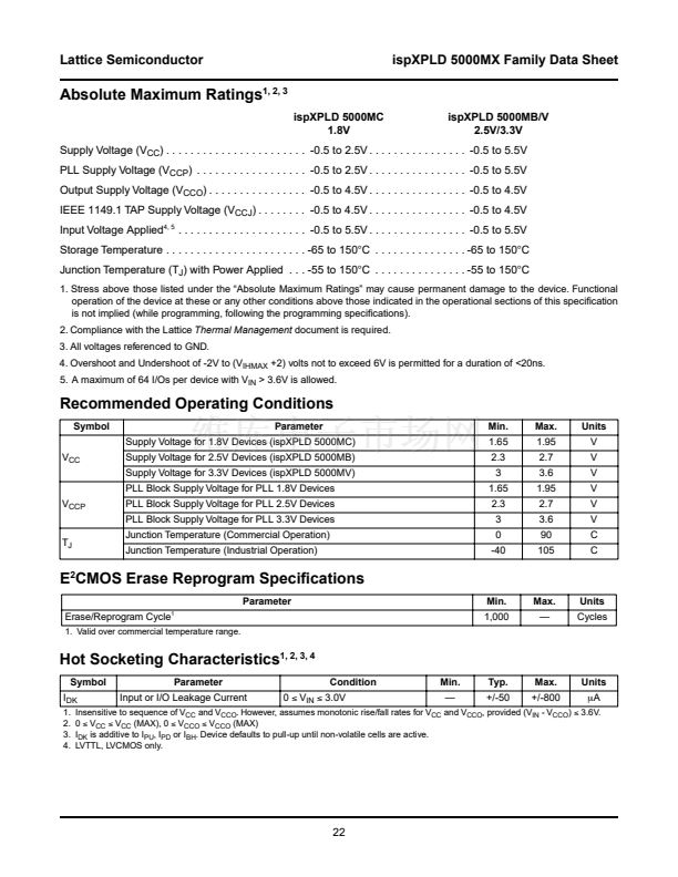
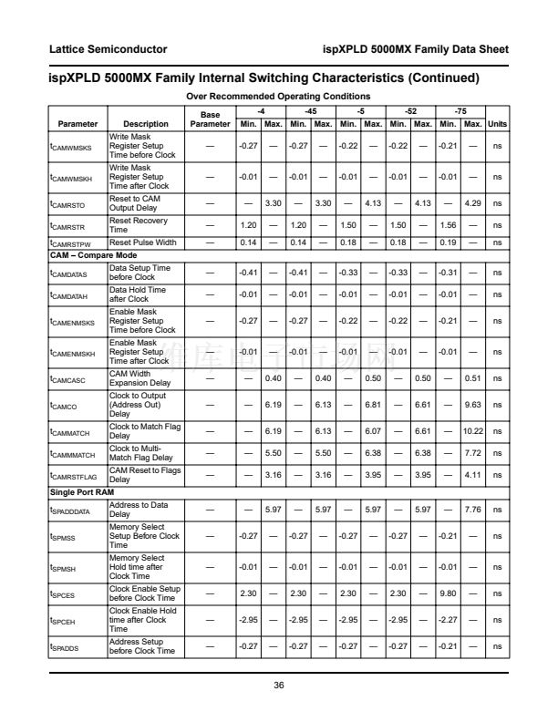
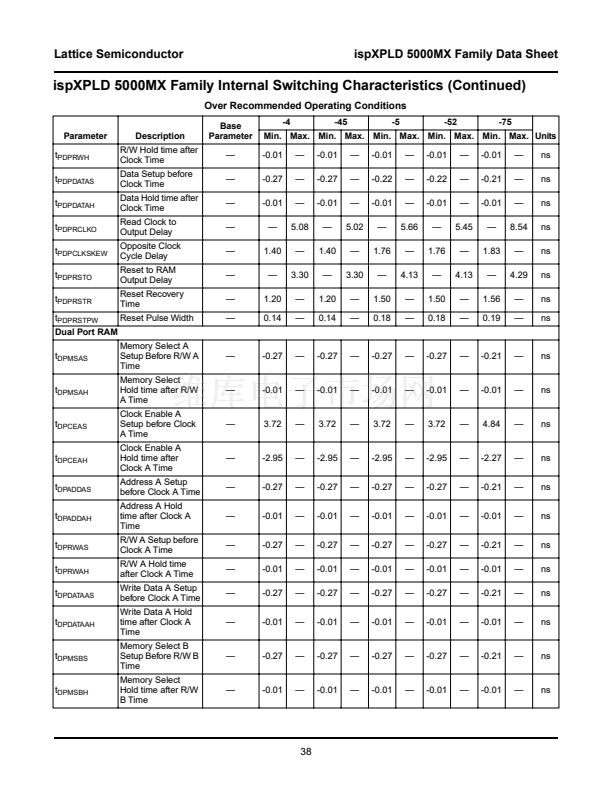
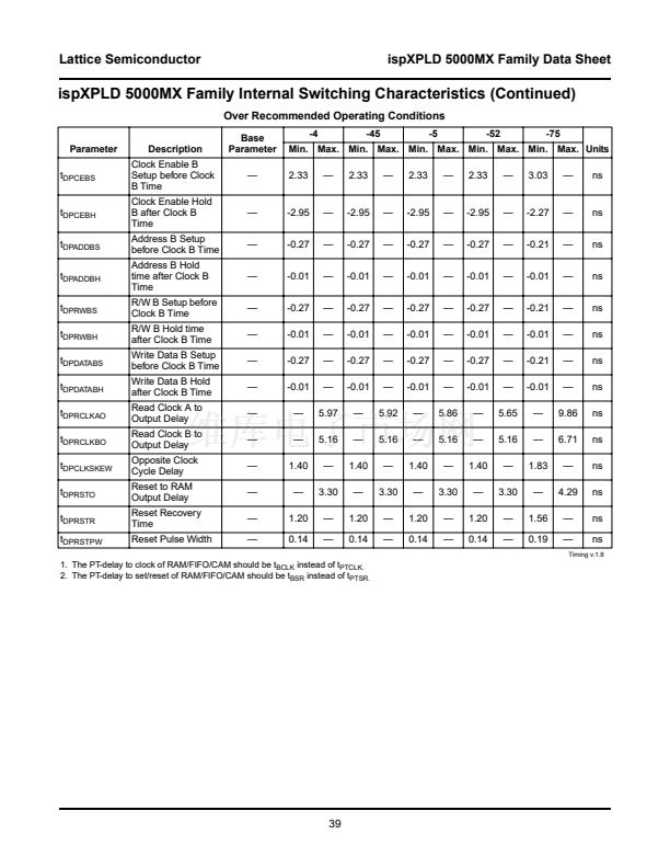
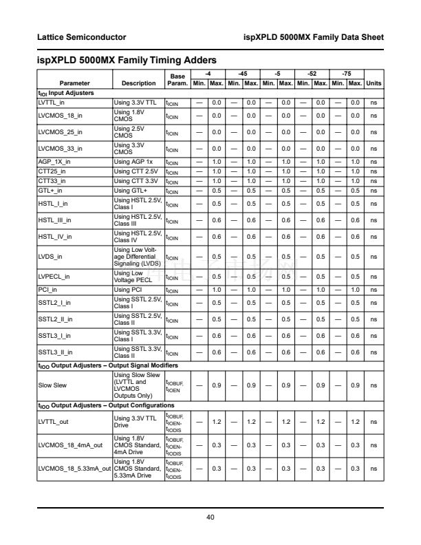
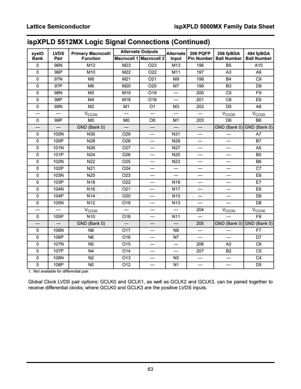
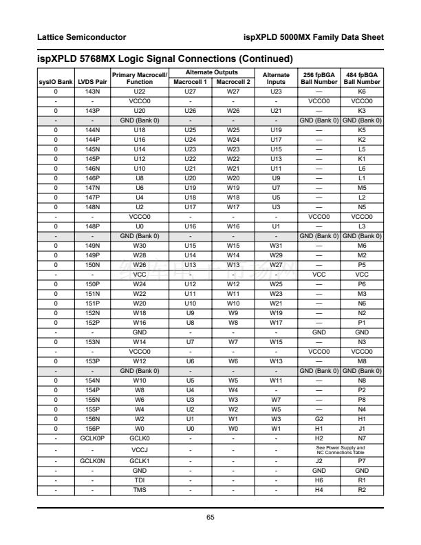
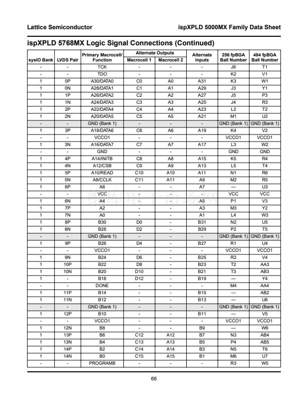
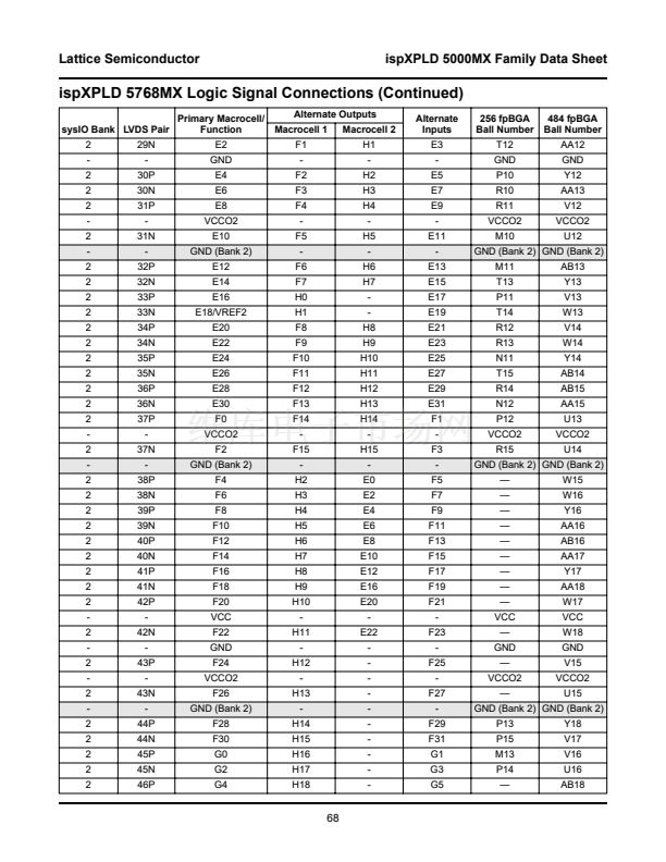
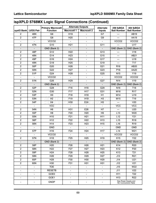
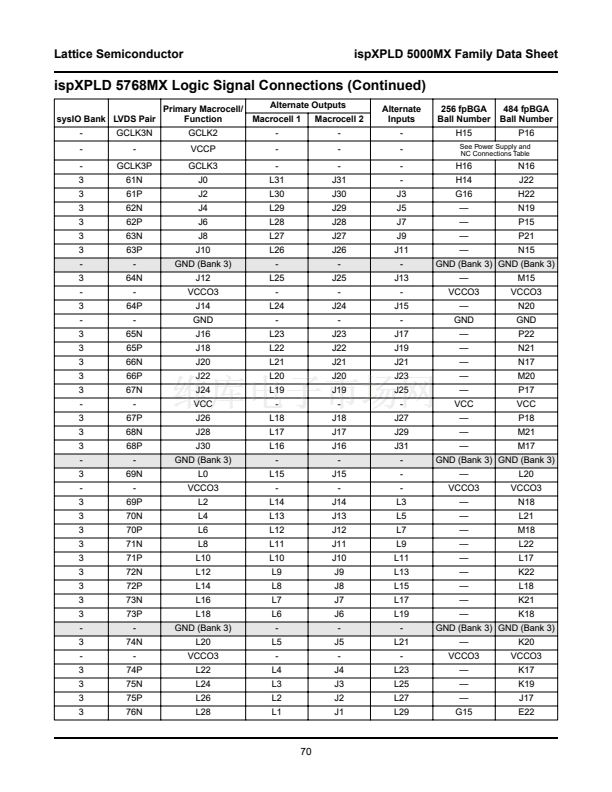
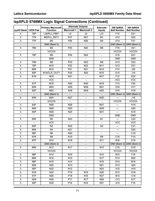
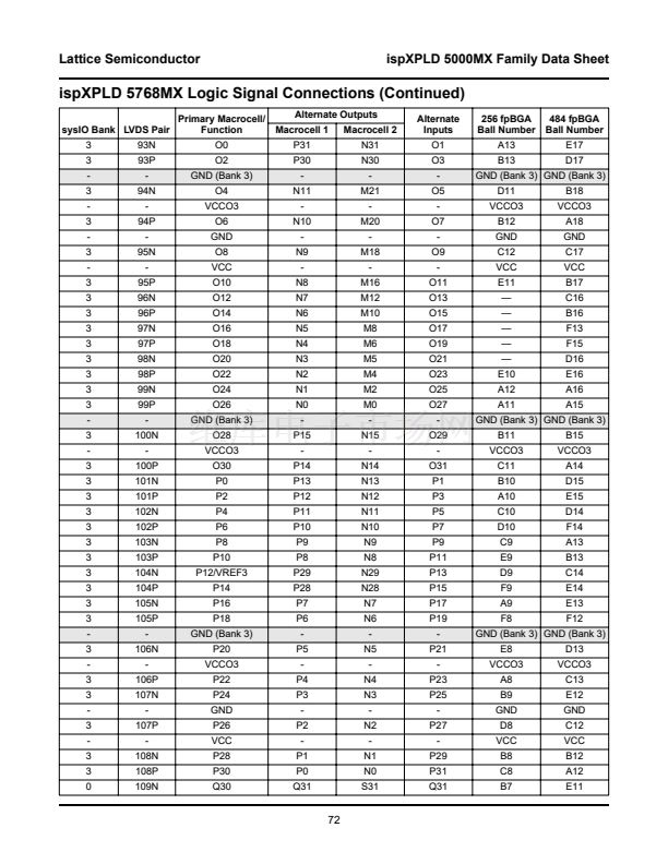
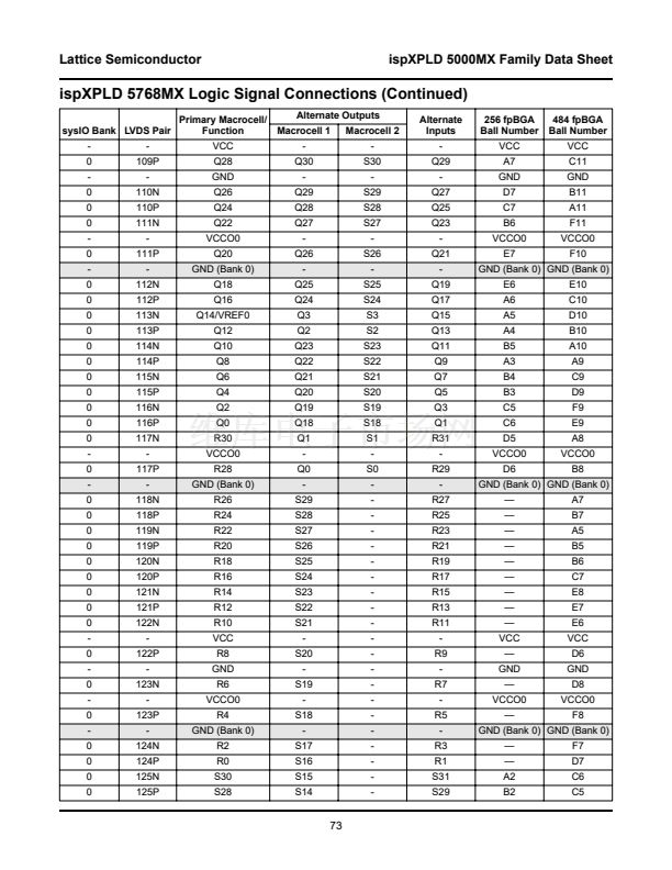
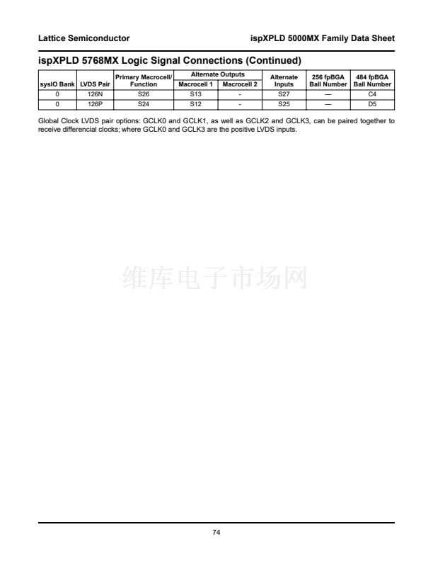
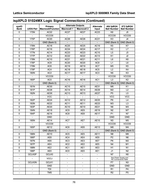
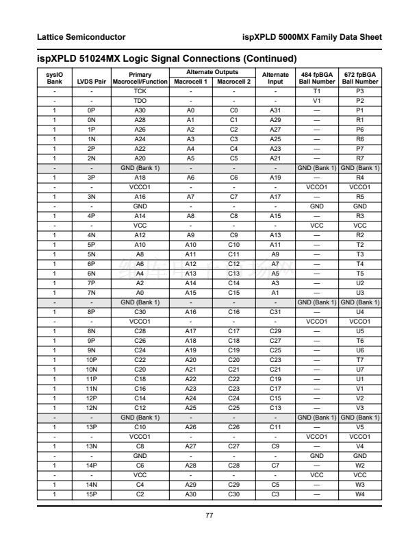
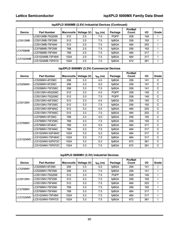
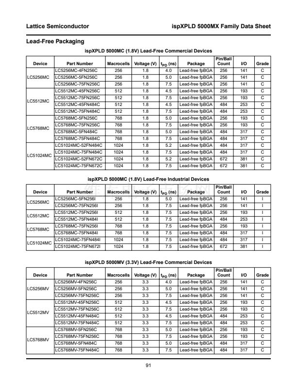
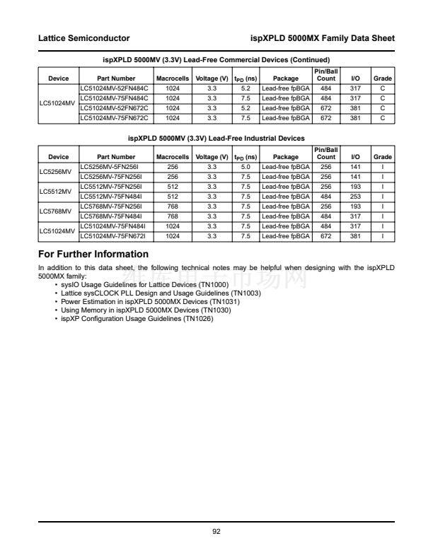
Lattice Semiconductor
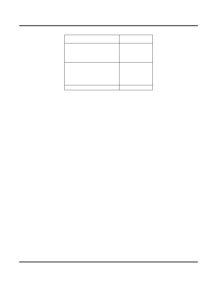
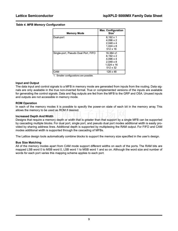
Table 4. MFB Memory Con铿乬uration
Memory Mode
Dual-port
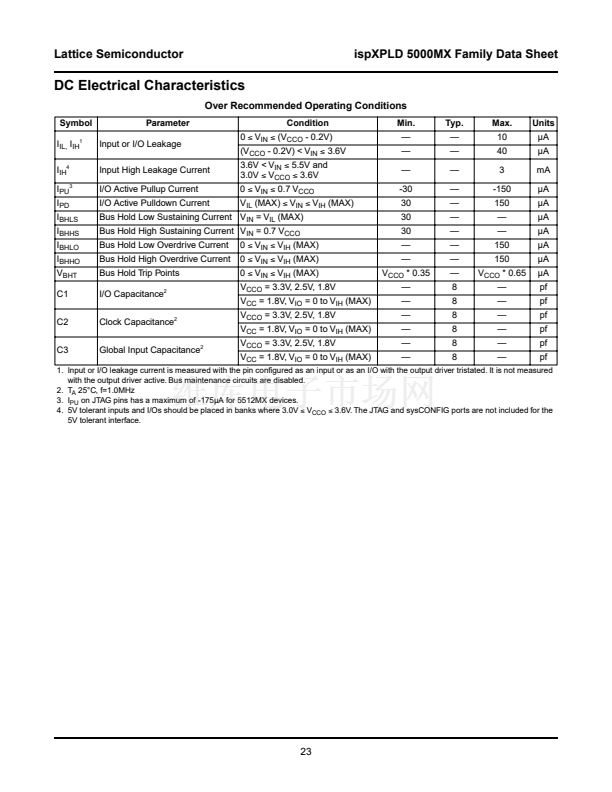
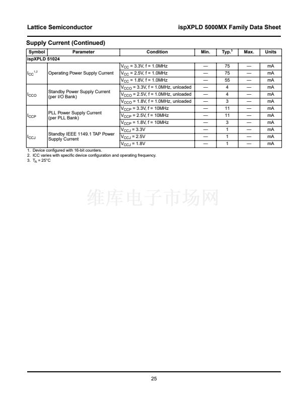
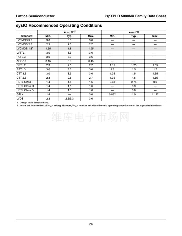
ispXPLD 5000MX Family Data Sheet
Max. Con铿乬uration
Size
1
8,192 x 1
4,096 x 2
2,048 x 4
1,024 x 8
512 x 16
16,384 x1
8,192 x 2
4,096 x 4
2,048 x 8
1,024 x 16
512 x 32
128 x 48
Single-port, Pseudo Dual Port, FIFO
CAM
1. Smaller con铿乬urations are possible.
Input and Output
The data input and control signals to a MFB in memory mode are generated from inputs from the routing. Data sig-
nals are only available in the true non-inverted format. True or complemented versions of the inputs are available
for generating the control signals. Data and 铿俛g outputs are fed from the MFB to the GRP and OSA. Unused inputs
and outputs are not accessible in memory mode.
ROM Operation
In each of the memory modes it is possible to specify the power-on state of each bit in the memory array. This
allows the memory to be used as ROM if desired.
Increased Depth And Width
Designs that require a memory depth or width that is greater than that support by a single MFB can be supported
by cascading multiple blocks. For dual port, single port, and pseudo dual port modes additional width is easily pro-
vided by sharing address lines. Additional depth is supported by multiplexing the RAM output. For FIFO and CAM
modes additional width is supported through the cascading of MFBs.
The Lattice design tools automatically combine blocks to support the memory size speci铿乪d in the user鈥檚 design.
Bus Size Matching
All of the memory modes apart from CAM mode support different widths on each of the ports. The RAM bits are
mapped LSB word 0 to MSB word 0, LSB word 1 to MSB word 1 and so on. Although the word size and number of
words for each port varies this mapping scheme applies to each port.
9


 1
1
 2
2
 3
3
 4
4
 5
5
 6
6
 7
7
 8
8
 9
9
 10
10
 11
11
 12
12
 13
13
 14
14
 15
15
 16
16
 17
17
 18
18
 19
19
 20
20
 21
21
 22
22
 23
23
 24
24
 25
25
 26
26
 27
27
 28
28
 29
29
 30
30
 31
31
 32
32
 33
33
 34
34
 35
35
 36
36
 37
37
 38
38
 39
39
 40
40
 41
41
 42
42
 43
43
 44
44
 45
45
 46
46
 47
47
 48
48
 49
49
 50
50
 51
51
 52
52
 53
53
 54
54
 55
55
 56
56
 57
57
 58
58
 59
59
 60
60
 61
61
 62
62
 63
63
 64
64
 65
65
 66
66
 67
67
 68
68
 69
69
 70
70
 71
71
 72
72
 73
73
 74
74
 75
75
 76
76
 77
77
 78
78
 79
79
 80
80
 81
81
 82
82
 83
83
 84
84
 85
85
 86
86
 87
87
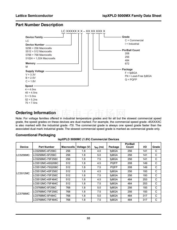 88
88
 89
89
 90
90
 91
91
 92
92
