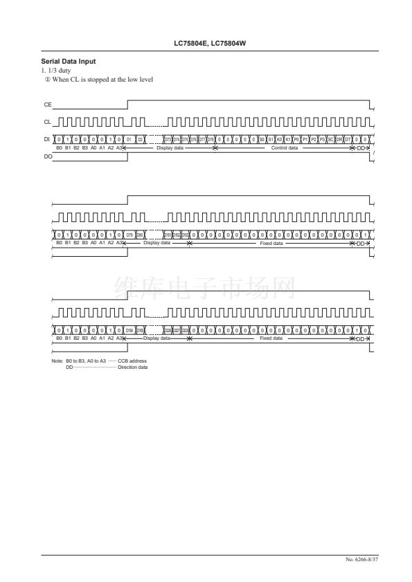
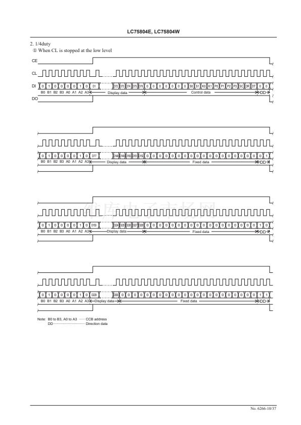
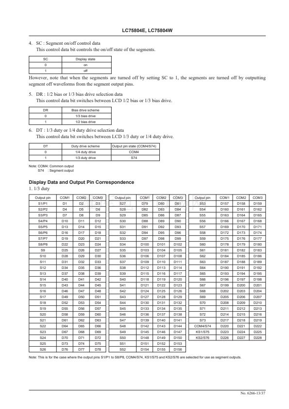
LC75804E, LC75804W
COM3
COM4/S74
COM1
COM2
S9
S8/P8
S2/P2
VLCD
VLCD1
VLCD2
VSS
TEST
OSC
DO
CLOCK
GENERATOR
CONTROL
REGISTER
COMMON
DRIVER
SHIFT REGISTER
SEGMENT DRIVER & LATCH
DI
CL
CE
VDD
VDET
CCB
INTERFACE
KEY BUFFER
KEY SCAN
RES
Blocks that are reset
3. Output pin states during the reset period
Output pin
S1/P1 to S8/P8
S9 to S73
COM1 to COM3
COM4/S74
KS1/S75, KS2/S76
KS3 to KS5
KS6
DO
State during reset
L
*5
L
L
L
*6
L
*5
X
*7
H
H
*8
X: don鈥檛 care
Notes:*5. These output pins are forcibly set to the segment output function and held low.
*6.
When power is first applied, this output pin is forcibly set to the common output function and held low. However, when the DT control data bit is
transferred, either the common output or the segment output function is selected.
*7.
When power is first applied, these output pins are undefined until the S0 and S1 control data bits have been transferred.
*8.
Since this output pin is an open-drain output, a pull-up resistor of between 1 and 10 k鈩?is required. This pin remains high during the reset period
even if a key data read operation is performed.
KS6
KS5
KS4
KS3
S76/KS2
S75/KS1
No. 6266-26/37
KI5
KI4
KI3
KI2
KI1
S1/P1
S73


 1
1
 2
2
 3
3
 4
4
 5
5
 6
6
 7
7
 8
8
 9
9
 10
10
 11
11
 12
12
 13
13
 14
14
 15
15
 16
16
 17
17
 18
18
 19
19
 20
20
 21
21
 22
22
 23
23
 24
24
 25
25
 26
26
 27
27
 28
28
 29
29
 30
30
 31
31
 32
32
 33
33
 34
34
 35
35
 36
36
 37
37
