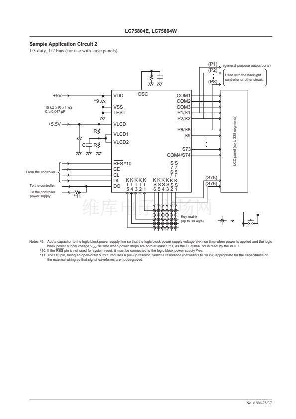
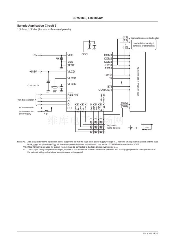
鈮?/div>
0.047 碌F
(general-purpose output ports)
Used with the backlight
controller or other circuit.
VDD
*9
VSS
TEST
VLCD
R
VLCD1
R
C
C
VLCD2
R
OSC
+5.5V
P8/S8
S9
From the controller
To the controller
To the controller
power supply
RES
*10
CE
CL
KKKKK
DI
DO I I I I I
54321
*11
S S S73
77
65
/ /
KKKKKK
SSSSSS
654321
(S75)
(S76)
Key matrix
(up to 30 keys)
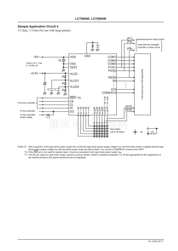
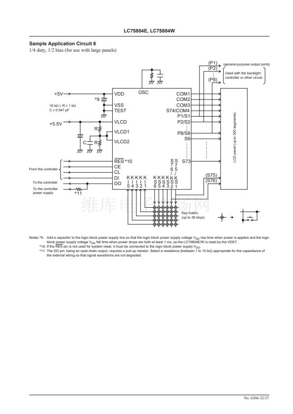
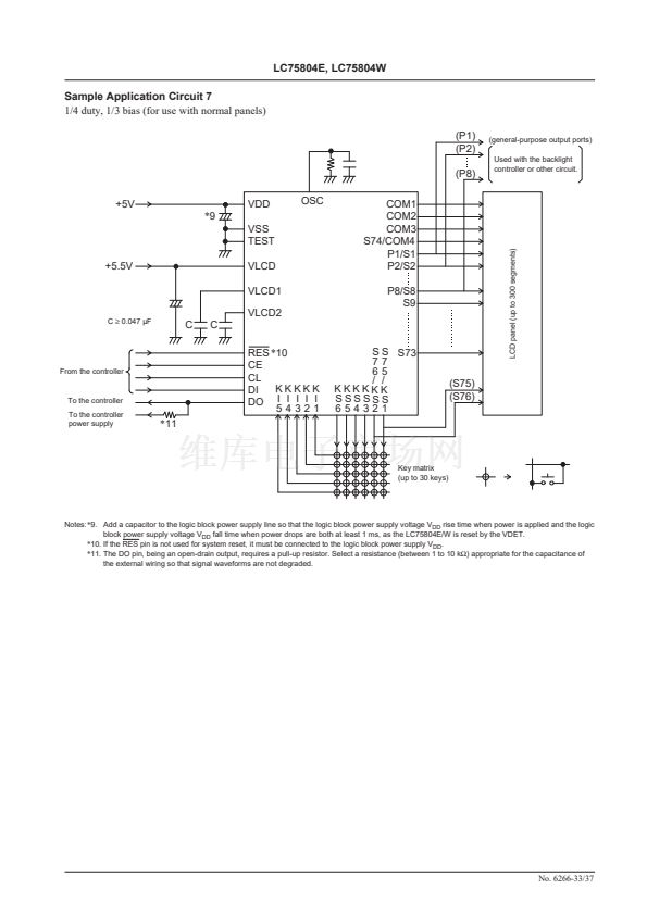
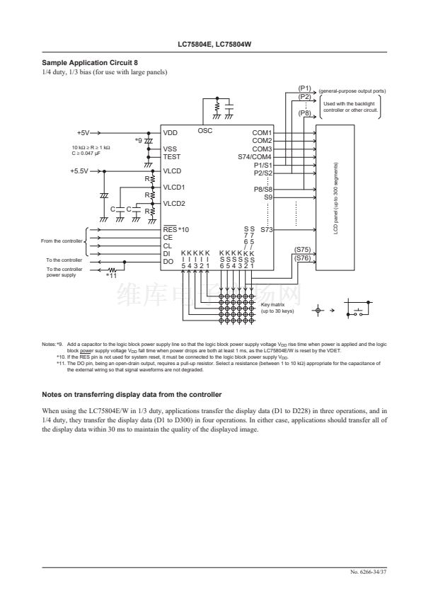
Notes:*9. Add a capacitor to the logic block power supply line so that the logic block power supply voltage V
DD
rise time when power is applied and the logic
block power supply voltage V
DD
fall time when power drops are both at least 1 ms, as the LC75804E/W is reset by the VDET.
*10.
If the RES pin is not used for system reset, it must be connected to the logic block power supply V
DD
.
*11.
The DO pin, being an open-drain output, requires a pull-up resistor. Select a resistance (between 1 to 10 k鈩? appropriate for the capacitance of
the external wiring so that signal waveforms are not degraded.
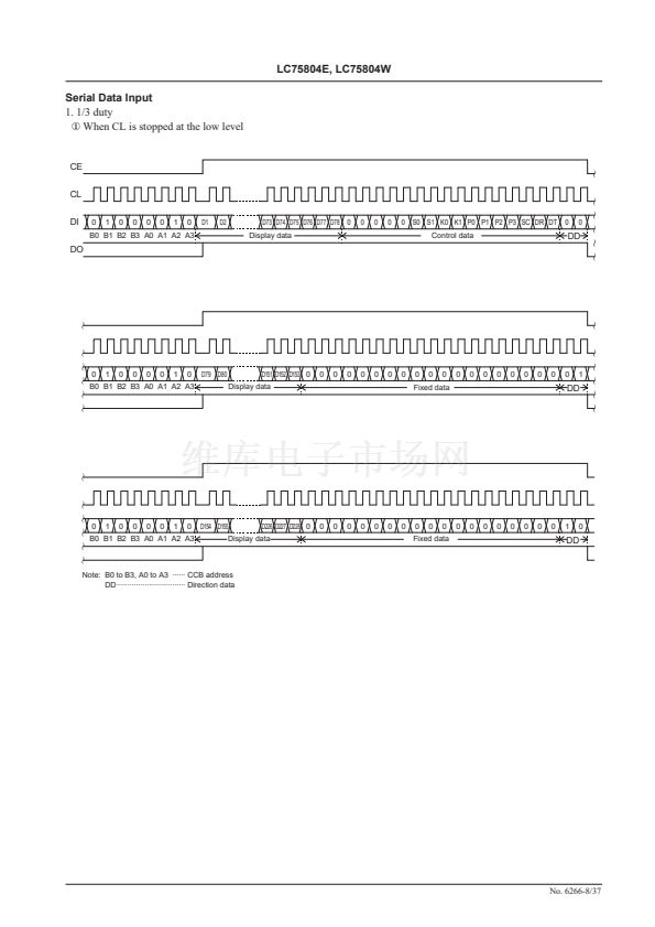
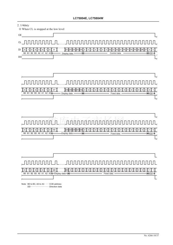
Notes on transferring display data from the controller
When using the LC75804E/W in 1/3 duty, applications transfer the display data (D1 to D228) in three operations, and in
1/4 duty, they transfer the display data (D1 to D300) in four operations. In either case, applications should transfer all of
the display data within 30 ms to maintain the quality of the displayed image.
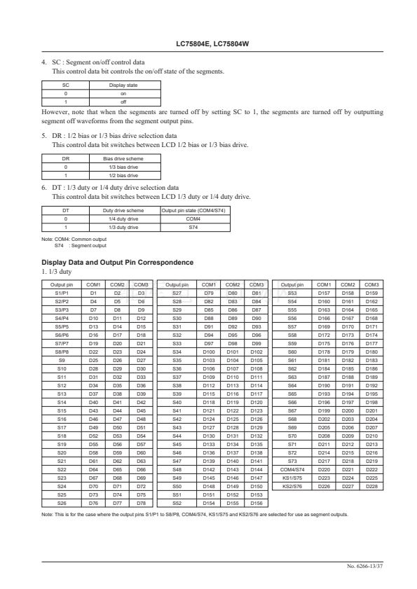
LCD panel (up to 300 segments)
COM1
COM2
COM3
S74/COM4
P1/S1
P2/S2
No. 6266-34/37


 1
1
 2
2
 3
3
 4
4
 5
5
 6
6
 7
7
 8
8
 9
9
 10
10
 11
11
 12
12
 13
13
 14
14
 15
15
 16
16
 17
17
 18
18
 19
19
 20
20
 21
21
 22
22
 23
23
 24
24
 25
25
 26
26
 27
27
 28
28
 29
29
 30
30
 31
31
 32
32
 33
33
 34
34
 35
35
 36
36
 37
37
