1鈩?/div>
脳
0.6 = 0.25W
P
REG
= 5V
脳
0.018A + 0.25 = 0.34W
Approximate diode power dissipation for boost and buck
converters is shown below. For other topologies or more
accurate results, see Application Note 19 or use
SwitcherCAD.
Boost: P
DIODE
= I
OUT
脳
V
f
Buck: P
DIODE
= I
OUT
脳
V
f
脳
(V
IN
鈥?V
OUT
)/V
IN
V
f
= diode forward voltage at a current equal to I
OUT
for a
buck converter and I
OUT
脳
V
OUT
/V
IN
for a boost converter.
In most applications, full load current is used to calculate
die temperature. However, if overload conditions must
also be accounted for, three approaches are possible.
First, if loss of regulated output is acceptable under
overload conditions, the internal
thermal limit
of the
LT1572 will protect the die in most applications by shut-
ting off switch current.
Thermal limit is not a tested
parameter,
however, and should be considered only for
noncritical applications with temporary overloads.
The second approach for lower current applications is to
leave the second switch emitter (E2) open. This increases
U
switch 鈥渙n鈥?resistance by 2:1, but reduces switch current
limit by 2:1 also, resulting in a net 2:1 reduction in I
2
R
switch dissipation under current limit conditions.
The third approach is to clamp the V
C
pin to a voltage less
than its internal clamp level of 2V. The LT1172 switch
current limit is zero at approximately 1V on the V
C
pin and
2A at 2V on the V
C
pin. Peak switch current can be
externally clamped between these two levels with a diode.
See AN19 for details.
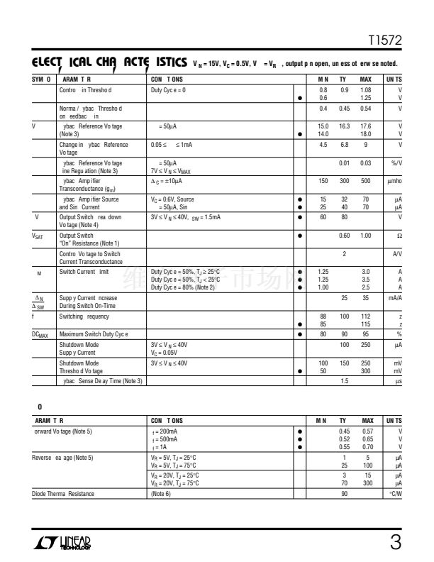
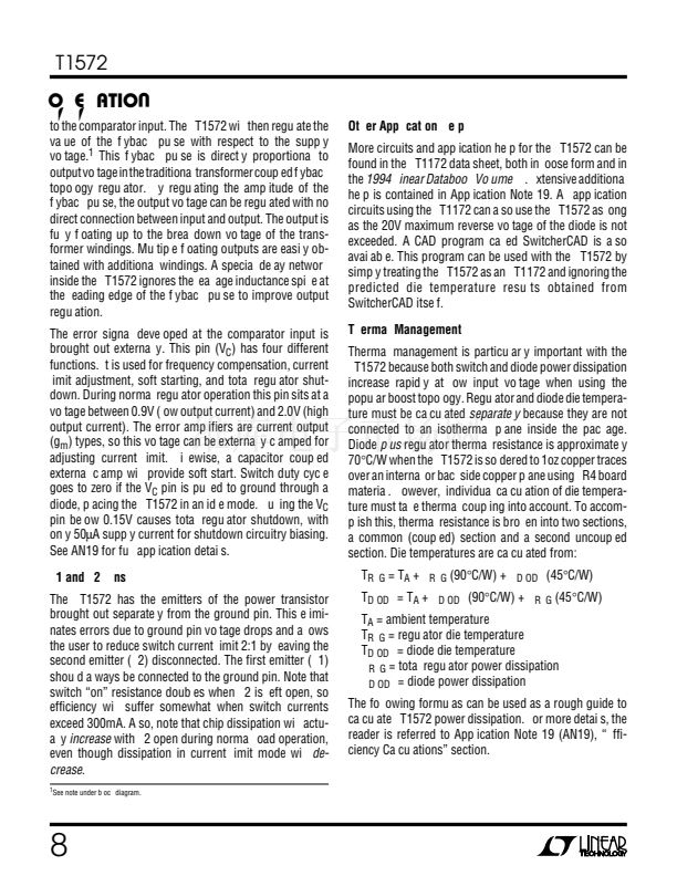
Diode Characteristics
The catch diode used in the LT1572 is a power Schottky
diode with a very low storage time and low forward
voltage. This gives good efficiency in switching regulator
applications, but some thought must be given to maxi-
mum operating voltage and high temperature reverse
leakage.
Peak repetitive reverse voltage rating on the diode
is 20V.
In a boost converter, maximum diode reverse
voltage is equal to regulated output voltage, so this limits
maximum output voltage to 20V. In a negative-to-positive
converter, maximum diode voltage will be equal to the
sum of output voltage
plus
input voltage. Use the equa-
tions in Application Note 19 or SwitcherCAD or calculate
maximum diode voltage for other topologies.
Diode reverse leakage increases rapidly with temperature.
This leakage is not high enough to significantly impact
efficiency or diode power dissipation, but it can be of
concern in shutdown mode if the diode is connected in
such a way that the leakage adds to regulator shutdown
current. Use the graphs of diode leakage versus voltage
and temperature to ensure proper high temperature sys-
tem performance.
The LT1572 diode is internally bonded to more than two
package pins to reduce internal bond wire currents.
All
pins must be used to prevent excessive current in the
individual internal bond wires.
This is important in low
load current applications because the LT1572 will draw
high surge currents during start-up (to charge the output
capacitor) even with no output load current.
9


 1
1
 2
2
 3
3
 4
4
 5
5
 6
6
 7
7
 8
8
 9
9
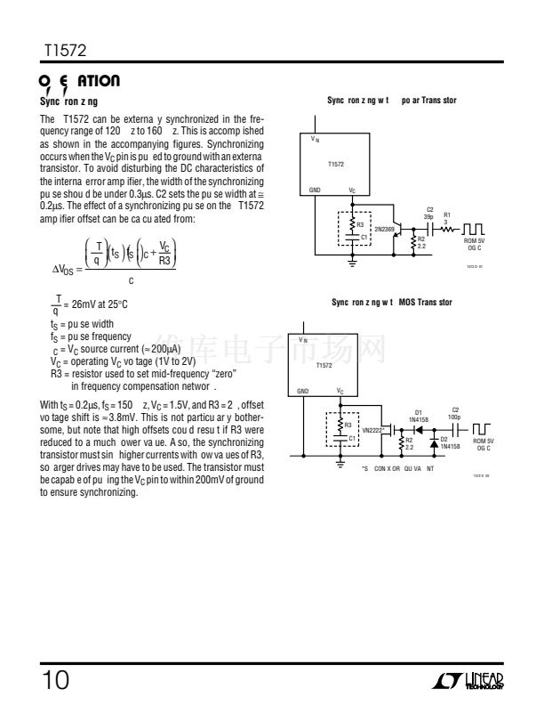 10
10
 11
11
 12
12
