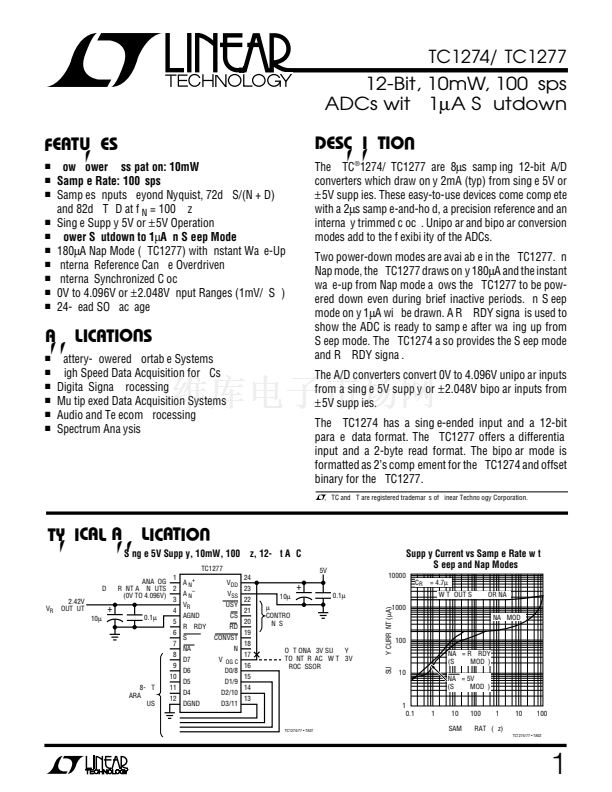
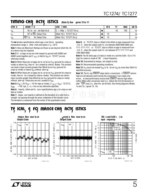
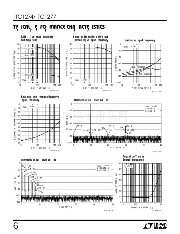
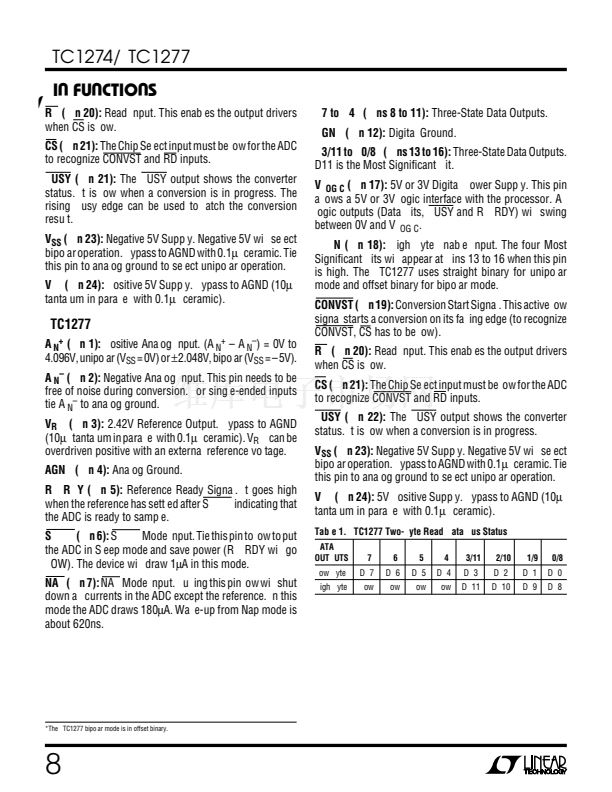
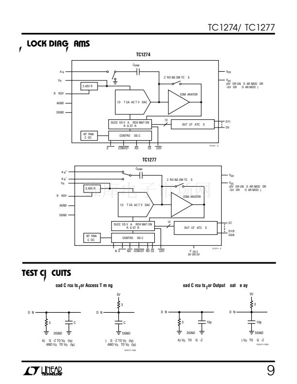
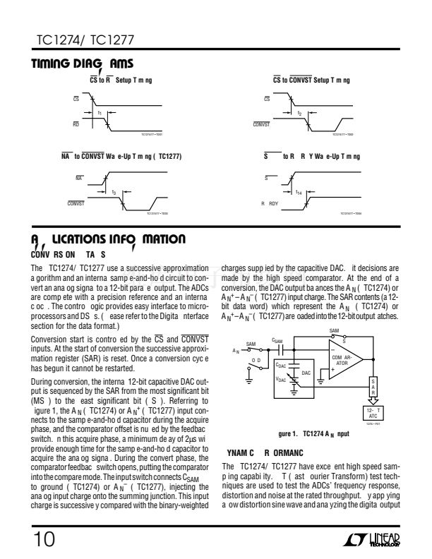
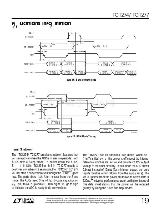
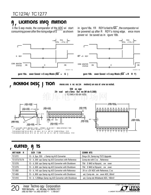
鈥?/div>
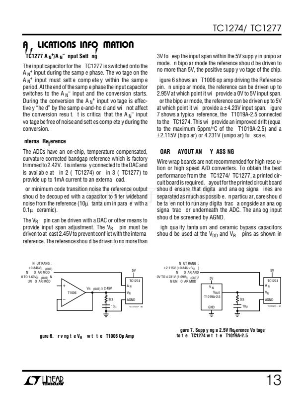
Figure 6. Driving the V
REF
with the LT1006 Op Amp
U
3V to keep the input span within the 5V supply in unipolar
mode. In bipolar mode the reference should be driven to
no more than 5V, the positive supply voltage of the chip.
Figure 6 shows an LT1006 op amp driving the Reference
pin. In unipolar mode, the reference can be driven up to
2.95V at which point it will provide a 0V to 5V input span.
For the bipolar mode, the reference can be driven up to 5V
at which point it will provide a
卤4.23V
input span. Figure
7 shows a typical reference, the LT1019A-2.5 connected
to the LTC1274. This will provide an improved drift (equal
to the maximum 5ppm/掳C of the LT1019A-2.5) and a
卤2.115V
(bipolar) or 4.231V (unipolar) full scale.
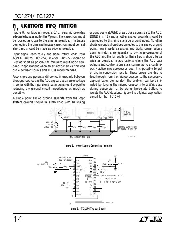
BOARD LAYOUT AND BYPASSING
Wire wrap boards are not recommended for high resolu-
tion or high speed A/D converters. To obtain the best
performance from the LTC1274/LTC1277, a printed cir-
cuit board is required. Layout for the printed circuit board
should ensure that digital and analog signal lines are
separated as much as possible. In particular, care should
be taken not to run any digital track alongside an analog
signal track or underneath the ADC. The analog input
should be screened by AGND.
High quality tantalum and ceramic bypass capacitors
should be used at the V
DD
and V
REF
pins as shown in
5V
W
U
UO
INPUT RANGE:
卤2.115V
(卤0.846
脳
V
REF
)
IN BIPOLAR AND
0V TO 4.231V (1.69V
REF(OUT)
)
IN UNIPOLAR MODE
5V
5V
V
IN
V
OUT
LT1019A-2.5
GND
3鈩?/div>
10碌F
LTC1274
A
IN
V
REF
AGND
LTC1274/77 鈥?F07
Figure 7. Supplying a 2.5V Reference Voltage
to the LTC1274 with the LT1019A-2.5
13


 1
1
 2
2
 3
3
 4
4
 5
5
 6
6
 7
7
 8
8
 9
9
 10
10
 11
11
 12
12
 13
13
 14
14
 15
15
 16
16
 17
17
 18
18
 19
19
 20
20
