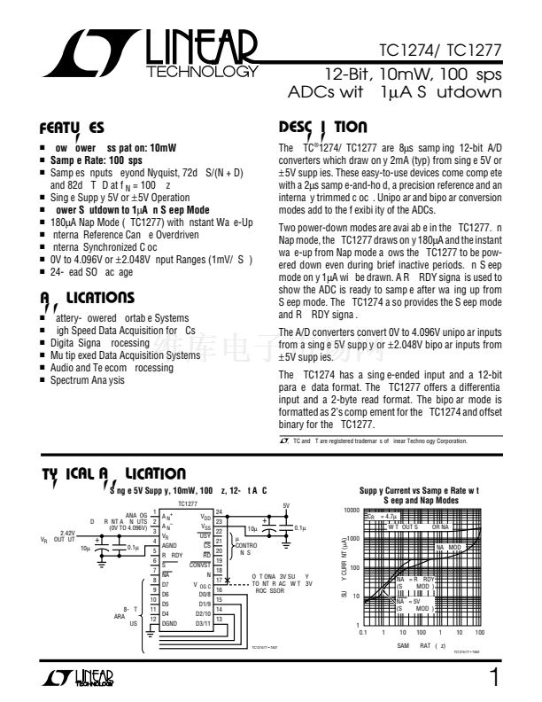
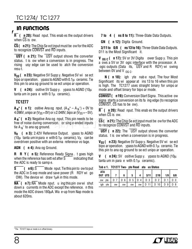
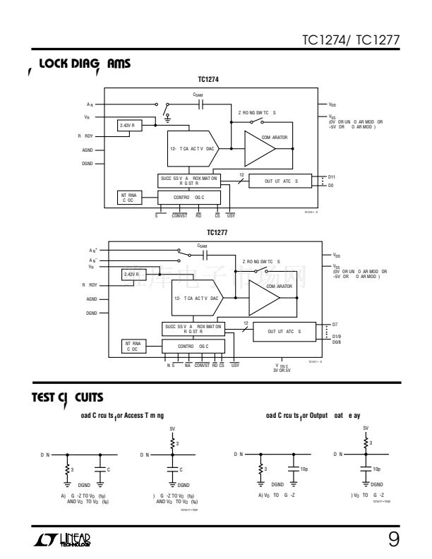
LTC1274/LTC1277
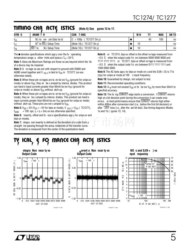
TI I G CHARACTERISTICS
SYMBOL
t
16
t
17
t
18
PARAMETER
HBEN鈫?to Low Byte Data Valid
HBEN鈫?to RD鈫?Setup Time
RD鈫?to HBEN鈫?Setup Time
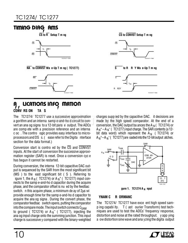
The
q
denotes specifications which apply over the full operating
temperature range; all other limits and typicals T
A
= 25掳C.
Note 1:
Absolute Maximum Ratings are those values beyond which the life
of a device may be impaired.
Note 2:
All voltage values are with respect to ground with DGND and
AGND wired together and V
LOGIC
is tied to V
DD
in LTC1277 (unless
otherwise noted).
Note 3:
When these pin voltages are taken below V
SS
(ground for unipolar
mode) or above V
DD
, they will be clamped by internal diodes. This product
can handle input currents greater than 60mA below V
SS
(ground for
unipolar mode) or above V
DD
without latch-up.
Note 4:
When these pin voltages are taken below V
SS
(ground for unipolar
mode), they will be clamped by internal diodes. This product can handle
input currents greater than 60mA below V
SS
(ground for unipolar mode)
without latch-up. These pins are not clamped to V
DD
.
Note 5:
V
DD
= 5V (V
SS
= 鈥?5V for bipolar mode), V
LOGIC
= V
DD
(LTC1277),
f
SAMPLE
= 100ksps, t
r
= t
f
= 5ns unless otherwise specified.
Note 6:
Linearity, offset and full-scale specifications apply for unipolar and
bipolar modes.
Note 7:
Integral nonlinearity is defined as the deviation of a code from a
straight line passing through the actual endpoints of the transfer curve.
The deviation is measured from the center of the quantization band.
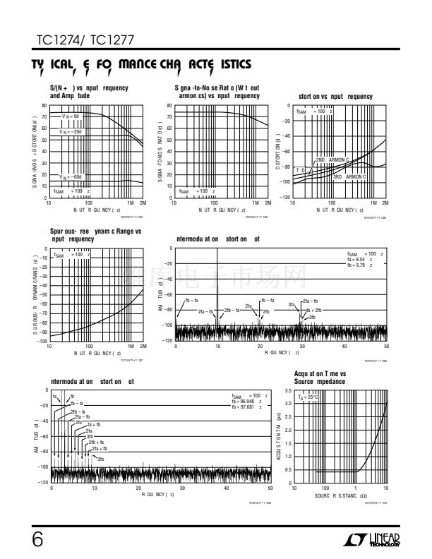
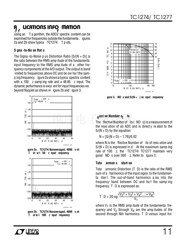
TYPICAL PERFORMANCE CHARACTERISTICS
Integral Nonlinearity vs
Output Code
DIFFERENTIAL NONLINEARITY ERROR (LSB)
1.00
INTEGRAL NONLINEARITY ERROR (LSB)
EFFECTIVE NUMBER OF BITS (ENOBs)
f
SAMPLE
= 100kHz
0.50
0
鈥?.50
鈥?.00
0
512 1024 1536 2048 2560 3072 3584 4096
OUTPUT CODE
LT1274/77 鈥?TPC01
U W
UW
(Note 5) See Figures 13 to 17.
MIN
q
q
q
CONDITIONS
C
L
= 100pF (LTC1277 Only)
(Note 10) (LTC1277 Only)
(Note 10) (LTC1277 Only)
TYP
45
MAX
100
UNITS
ns
ns
ns
10
10
Note 8:
For LTC1274, bipolar offset is the offset voltage measured from
鈥?0.5LSB when the output code flickers between 0000 0000 0000 and
1111 1111 1111. For LTC1277, bipolar offset voltage is measured from
鈥?0.5LSB when the output code flickers between 0111 1111 1111 and
1000 0000 0000.
Note 9:
The AC tests apply to bipolar mode only and the S/(N + D) is 71dB
(typ) for unipolar mode at 100kHz input frequency.
Note 10:
Guaranteed by design, not subject to test.
Note 11:
Recommended operating conditions.
Note 12:
A
IN
must not exceed V
DD
or fall below V
SS
by more than 50mV to
specified accuracy.
Note 13:
The falling CONVST edge starts a conversion. If CONVST returns
high at a bit decision point during the conversion it can create small
errors. For best performance ensure that CONVST returns high either
within 400ns after conversion start (i.e., before the first bit decision) or
after BUSY rises (i.e., after the last bit test). See timing diagrams Modes
1a and 1b (Figures 13, 14).
Differential Nonlinearity vs
Output Code
1.00
f
SAMPLE
= 100kHz
0.50
12
11
10
9
8
7
6
5
4
3
2
1
ENOBs and S/(N + D) vs
Input Frequency
74
68
NYQUIST
FREQUENCY
62
56
50
S/(N + D)(dB)
0
鈥?.50
f
SAMPLE
= 100kHz
100k
INPUT FREQUENCY (Hz)
1M
2M
鈥?.00
0
512 1024 1536 2048 2560 3072 3584 4096
OUTPUT CODE
LT1274/77 鈥?TPC02
0
10k
LTC1274/77 鈥?TPC03
5


 1
1
 2
2
 3
3
 4
4
 5
5
 6
6
 7
7
 8
8
 9
9
 10
10
 11
11
 12
12
 13
13
 14
14
 15
15
 16
16
 17
17
 18
18
 19
19
 20
20
