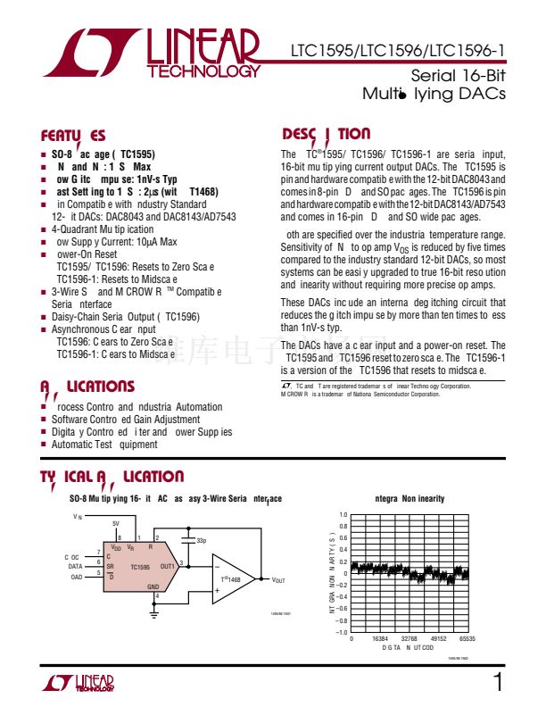
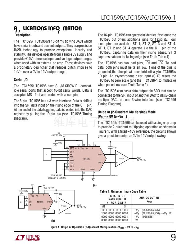
LTC1595/LTC1596/LTC1596-1
ELECTRICAL CHARACTERISTICS
SYMBOL
t
SRI
t
CH
t
CL
t
LD
t
ASB
PARAMETER
Serial Input Data Pulse Width
Clock Pulse Width High
Clock Pulse Width Low
Load Pulse Width
LSB Clocked into Input Register
to DAC Register Load Time
CONDITIONS
q
q
q
q
q
MIN
60
60
60
60
0
TYP
MAX
UNITS
ns
ns
ns
ns
ns
V
DD
= 5V
卤10%,
V
REF
= 10V, V
OUT1
= V
OUT2
= AGND = 0V, T
A
= T
MIN
to T
MAX
, unless otherwise noted.
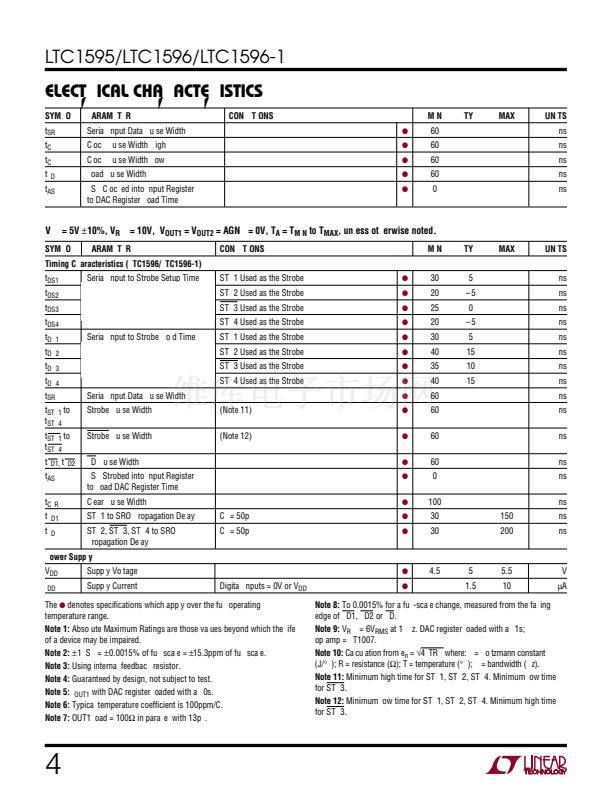
SYMBOL
t
DS1
t
DS2
t
DS3
t
DS4
t
DH1
t
DH2
t
DH3
t
DH4
t
SRI
t
STB1
to
t
STB4
t
STB1
to
t
STB4
t
LD1,
t
LD2
t
ASB
t
CLR
t
PD1
t
PD
Serial Input Data Pulse Width
Strobe Pulse Width
Strobe Pulse Width
LD Pulse Width
LSB Strobed into Input Register
to Load DAC Register Time
Clear Pulse Width
STB1 to SRO Propagation Delay
STB2, STB3, STB4 to SRO
Propagation Delay
Supply Voltage
Supply Current
Digital Inputs = 0V or V
DD
C
L
= 50pF
C
L
= 50pF
(Note 11)
(Note 12)
Serial Input to Strobe Hold Time
PARAMETER
Serial Input to Strobe Setup Time
CONDITIONS
STB1 Used as the Strobe
STB2 Used as the Strobe
STB3 Used as the Strobe
STB4 Used as the Strobe
STB1 Used as the Strobe
STB2 Used as the Strobe
STB3 Used as the Strobe
STB4 Used as the Strobe
q
q
q
q
q
q
q
q
q
q
q
q
q
q
q
q
MIN
30
20
25
20
30
40
35
40
60
60
60
60
0
100
30
30
TYP
5
鈥?
0
鈥?
5
15
10
15
MAX
UNITS
ns
ns
ns
ns
ns
ns
ns
ns
ns
ns
ns
ns
ns
ns
Timing Characteristics (LTC1596/LTC1596-1)
150
200
ns
ns
Power Supply
V
DD
I
DD
q
q
4.5
5
1.5
5.5
10
V
碌A
The
q
denotes specifications which apply over the full operating
temperature range.
Note 1:
Absolute Maximum Ratings are those values beyond which the life
of a device may be impaired.
Note 2:
卤1LSB
=
卤0.0015%
of full scale =
卤15.3ppm
of full scale.
Note 3:
Using internal feedback resistor.
Note 4:
Guaranteed by design, not subject to test.
Note 5:
I
OUT1
with DAC register loaded with all 0s.
Note 6:
Typical temperature coefficient is 100ppm/C.
Note 7:
OUT1 load = 100鈩?in parallel with 13pF.
Note 8:
To 0.0015% for a full-scale change, measured from the falling
edge of LD1, LD2 or LD.
Note 9:
V
REF
= 6V
RMS
at 1kHz. DAC register loaded with all 1s;
op amp = LT1007.
Note 10:
Calculation from e
n
=
鈭?kTRB
where: k = Boltzmann constant
(J/掳K); R = resistance (鈩?; T = temperature (掳K); B = bandwidth (Hz).
Note 11:
Minimum high time for STB1, STB2, STB4. Minimum low time
for STB3.
Note 12:
Minimum low time for STB1, STB2, STB4. Minimum high time
for STB3.
4


 1
1
 2
2
 3
3
 4
4
 5
5
 6
6
 7
7
 8
8
 9
9
 10
10
 11
11
 12
12
