鈮?/div>
5.5V.
Requires a bypass capacitor to ground.
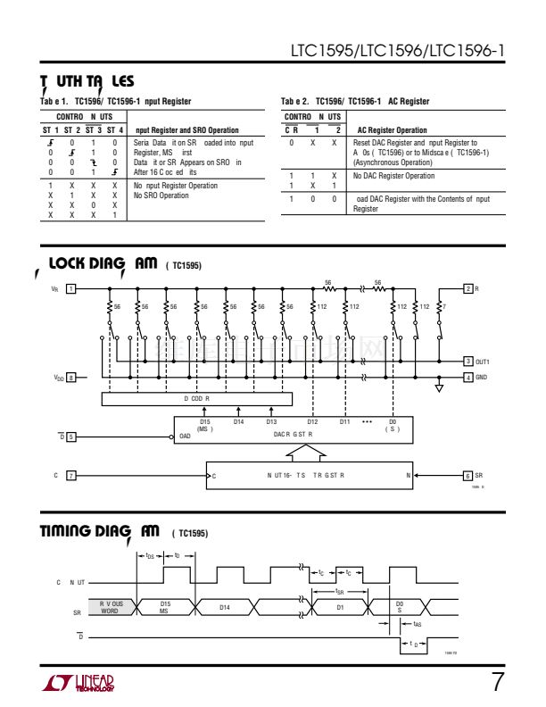
STB1, STB2, STB3, STB4 (Pins 4, 8, 10, 11):
Serial
Interface Clock Inputs. STB1, STB2 and STB4 are rising
edge triggered inputs. STB3 is a falling edge triggered
input (see Truth Tables).
LD1, LD2 (Pins 5, 9):
Serial Interface Load Control Inputs.
When LD1 and LD2 are pulled low, data is loaded from the
shift register into the DAC register, updating the DAC
output (see Truth Tables).
SRO (Pin 6):
The Output of the Shift Register. Becomes
valid on the active edge of the serial clock.
SRI (Pin 7):
The Serial Data Input. Data on the SRI pin is
latched into the shift register on the active edge of the
serial clock. Data is loaded MSB first.
DGND (Pin 12):
Digital Ground Pin.
CLR (Pin 13):
The Clear Pin for the DAC. Clears DAC to zero
scale when pulled low on LTC1596. Clears DAC to midscale
when pulled low on LTC1596-1. This pin should be tied to
V
DD
for normal operation.
V
DD
(Pin 14):
The Positive Supply Input. 4.5V
鈮?/div>
V
DD
鈮?/div>
5.5V. Requires a bypass capacitor to ground.
V
REF
(Pin 15):
Reference Input.
R
FB
(Pin 16):
Feedback Resistor. Normally tied to the
output of the current to voltage converter op amp.
LTC1596/LTC1596-1
OUT1 (Pin 1):
True Current Output Pin. Tie to inverting
input of current to voltage converter op amp.
OUT2 (Pin 2):
Complement Current Output Pin. Tie to
analog ground.
AGND (Pin 3):
Analog Ground Pin.
6
U W
Logic Threshold
vs Supply Voltage
3.0
2.5
2.0
1.5
1.0
0.5
0
3
2
INPUT VOLTAGE (V)
4
5
1595/96 G10
0
1
2
3 4 5 6 7 8
SUPPLY VOLTAGE (V)
9
10
1595/96 G11
U
U
U


 1
1
 2
2
 3
3
 4
4
 5
5
 6
6
 7
7
 8
8
 9
9
 10
10
 11
11
 12
12
