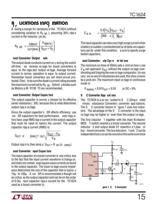
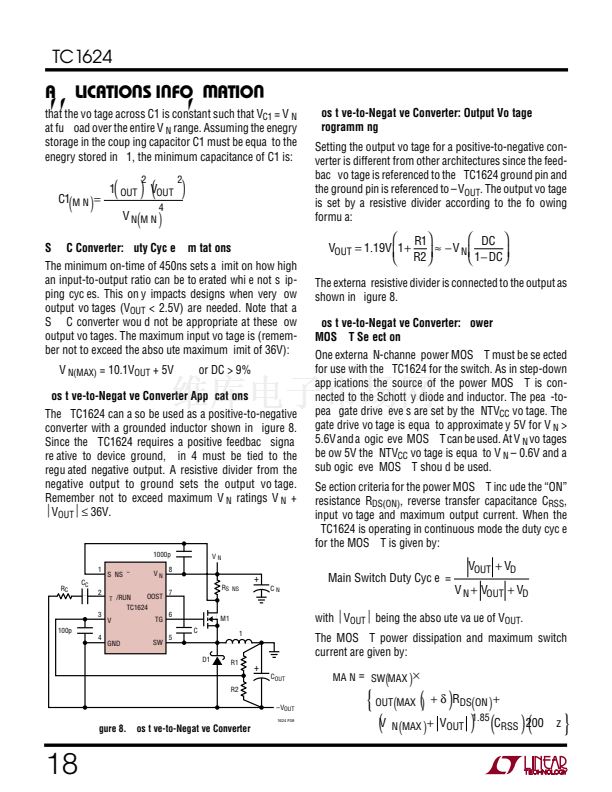
LTC1624
APPLICATIONS INFORMATION
what is limiting the efficiency and which change would
produce the most improvement. Percent efficiency can be
expressed as:
%Efficiency = 100% 鈥?(L1 + L2 + L3 + ...)
where L1, L2, etc. are the individual losses as a percentage
of input power.
Although all dissipative elements in the circuit produce
losses, four main sources usually account for most of the
losses in LTC1624 circuits:
1. LTC1624 V
IN
current
2. I
2
R losses
3. Topside MOSFET transition losses
4. Voltage drop of the Schottky diode
1. The V
IN
current is the sum of the DC supply current I
Q
,
given in the Electrical Characteristics table, and the
MOSFET driver and control currents. The MOSFET
driver current results from switching the gate
capacitance of the power MOSFET. Each time a MOSFET
gate is switched from low to high to low again, a packet
of charge dQ moves from INTV
CC
to ground. The
resulting dQ/dt is a current out of V
IN
which is typically
much larger than the control circuit current. In
continuous mode, I
GATECHG
= f (Q
T
+ Q
B
), where Q
T
and
Q
B
are the gate charges of the topside and internal
bottom side MOSFETs.
By powering BOOST from an output-derived source
(Figure 10 application), the additional V
IN
current
resulting from the topside driver will be scaled by a
factor of (Duty Cycle)/(Efficiency). For example, in a
20V to 5V application, 5mA of INTV
CC
current results in
approximately 1.5mA of V
IN
current. This reduces the
midcurrent loss from 5% or more (if the driver was
powered directly from V
IN
) to only a few percent.
2. I
2
R losses are predicted from the DC resistances of the
MOSFET, inductor and current shunt. In continuous
mode the average output current flows through L but is
鈥渃hopped鈥?between the topside main MOSFET/current
shunt and the Schottky diode. The resistances of the
topside MOSFET and R
SENSE
multiplied by the duty
cycle can simply be summed with the resistance of L to
obtain I
2
R losses. (Power is dissipated in the sense
resistor only when the topside MOSFET is on. The I
2
R
loss is thus reduced by the duty cycle.) For example, at
50% DC, if R
DS(ON)
= 0.05鈩? R
L
= 0.15鈩?and R
SENSE
=
0.05鈩? then the effective total resistance is 0.2鈩? This
results in losses ranging from 2% to 8% for V
OUT
= 5V
as the output current increases from 0.5A to 2A. I
2
R
losses cause the efficiency to drop at high output
currents.
3. Transition losses apply only to the topside MOSFET(s),
and only when operating at high input voltages (typically
20V or greater). Transition losses can be estimated
from:
Transition Loss = 2.5(V
IN
)
1.85
(I
MAX
)(C
RSS
)(f)
4. The Schottky diode is a major source of power loss at
high currents and gets worse at high input voltages.
The diode loss is calculated by multiplying the forward
voltage drop times the diode duty cycle multiplied by
the load current. For example, assuming a duty cycle of
50% with a Schottky diode forward voltage drop of
0.5V, the loss is a relatively constant 5%.
As expected, the I
2
R losses and Schottky diode loss
dominate at high load currents. Other losses including
C
IN
and C
OUT
ESR dissipative losses and inductor core
losses generally account for less than 2% total additional
loss.
Checking Transient Response
The regulator loop response can be checked by looking at
the load transient response. Switching regulators take
several cycles to respond to a step in DC (resistive) load
current. When a load step occurs, V
OUT
immediately shifts
by an amount equal to (鈭咺
LOAD
鈥?ESR), where ESR is the
effective series resistance of C
OUT
.
鈭咺
LOAD
also begins to
charge or discharge C
OUT
which generates a feedback
error signal. The regulator loop then acts to return V
OUT
to
its steady-state value. During this recovery time V
OUT
can
be monitored for overshoot or ringing that would indicate
a stability problem. The I
TH
external components shown in
the Figure 1 circuit will provide adequate compensation for
most applications.
A second, more severe transient, is caused by switching in
loads with large (>1碌F) supply bypass capacitors. The
discharged bypass capacitors are effectively put in parallel
U
W
U
U
11


 1
1
 2
2
 3
3
 4
4
 5
5
 6
6
 7
7
 8
8
 9
9
 10
10
 11
11
 12
12
 13
13
 14
14
 15
15
 16
16
 17
17
 18
18
 19
19
 20
20
 21
21
 22
22
 23
23
 24
24
 25
25
 26
26
 27
27
 28
28
