鈥?/div>
pin. This offset
cancels the internal offset in current comparator I
2
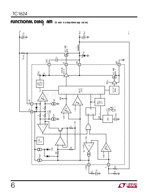
(refer
to Functional Diagram). This comparator in conjunction
with the voltage on the I
TH
/RUN pin determines when to
enter into Burst Mode operation (refer to Low Current
Operation in Operation section). With the additional exter-
nal offset present, the drive to the topside MOSFET is
always enabled every cycle and constant frequency opera-
tion occurs for I
OUT
> I
OUT(MIN)
.
Step-Down Converter: Design Example
As a design example, assume V
IN
= 12V(nominal),
V
IN
= 22V(max), V
OUT
= 3.3V and I
MAX
= 2A. R
SENSE
can
immediately be calculated:
R
SENSE
= 100mV/2A = 0.05鈩?/div>
Assume a 10碌H inductor. To check the actual value of the
ripple current the following equation is used:
With the 0.05鈩?sense resistor I
SC(AVG)
= 2A will result,
increasing the 0.5V Schottky diode dissipation to 0.98W.
C
IN
is chosen for an RMS current rating of at least 1.0A at
temperature. C
OUT
is chosen with an ESR of 0.03鈩?for low
output ripple. The output ripple in continuous mode will be
highest at the maximum input voltage. The output voltage
ripple due to ESR is approximately:
V
ORIPPLE
= R
ESR
(鈭咺
L
) = 0.03鈩?(1.58A
P-P
) = 47mV
P-P
Step-Down Converter: Duty Cycle Limitations
At high input to output differential voltages the on-time
gets very small. Due to internal gate delays and response
times of the internal circuitry the minimum recommended
on-time is 450ns. Since the LTC1624鈥檚 frequency is inter-
nally set to 200kHz a potential duty cycle limitation exists.
When the duty cycle is less than 9%, cycle skipping may
occur which increases the inductor ripple current but does
not cause V
OUT
to lose regulation. Avoiding cycle skipping
imposes a limit on the input voltage for a given output
voltage only when V
OUT
< 2.2V using 30V MOSFETs.
(Remember not to exceed the absolute maximum voltage
of 36V.)
V
IN(MAX)
= 11.1V
OUT
+ 5V
For DC > 9%
V
IN
鈭?/div>
V
OUT
铮?/div>
V
OUT
+
V
D
铮?/div>
鈭咺
L
=
铮?/div>
铮?/div>
f L
铮?/div>
V
IN
+
V
D
铮?/div>
( )( )
The highest value of the ripple current occurs at the
maximum input voltage:
鈭咺
L
=
22V
鈭?/div>
3
.
3V
铮?/div>
3
.
3V
+
0
.
5V
铮?/div>
铮?/div>
22V
+
0
.
5V
铮?=
1
.
58A
P-P
铮?/div>
200kHz 10
碌
H
铮?/div>
(
)
The power dissipation on the topside MOSFET can be
easily estimated. Choosing a Siliconix Si4412DY results
in: R
DS(ON)
= 0.042鈩? C
RSS
= 100pF. At maximum input
voltage with T(estimated) = 50掳C:
P
MAIN
=
2
3
.
3V
+
0
.
5V
2A 1
+
0
.
005 50
掳
C
鈭?/div>
25
掳
C 0
.
042
鈩?/div>
22V
+
0
.
5V
( )
[
( )(
)
]
(
1
.
85
+
2
.
5
(
22V
) (
2A
)(
100pF
)(
200kHz
)
=
62mW
铮?/div>
V
IN
铮?/div>
P
D
=
I
SC AVG
V
D
铮?/div>
铮?/div>
铮?/div>
V
IN
+
V
D
铮?/div>
The most stringent requirement for the Schottky diode
occurs when V
OUT
= 0V (i.e. short circuit) at maximum V
IN
.
In this case the worst-case dissipation rises to:
( )
(
)
U
W
U
U
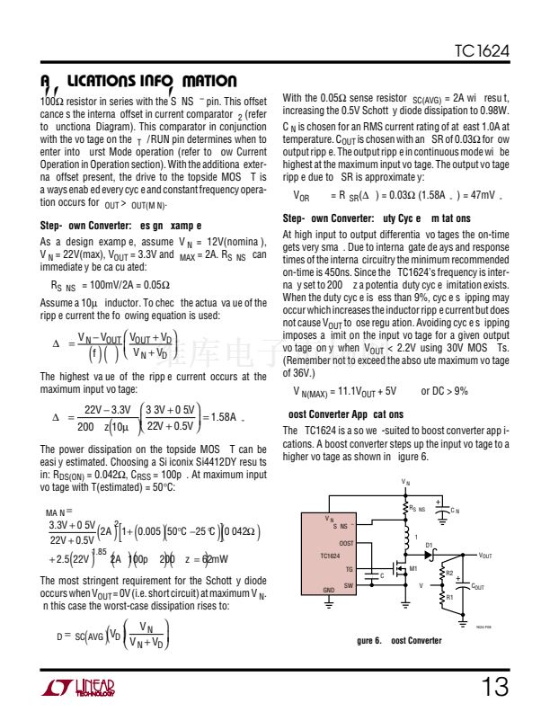
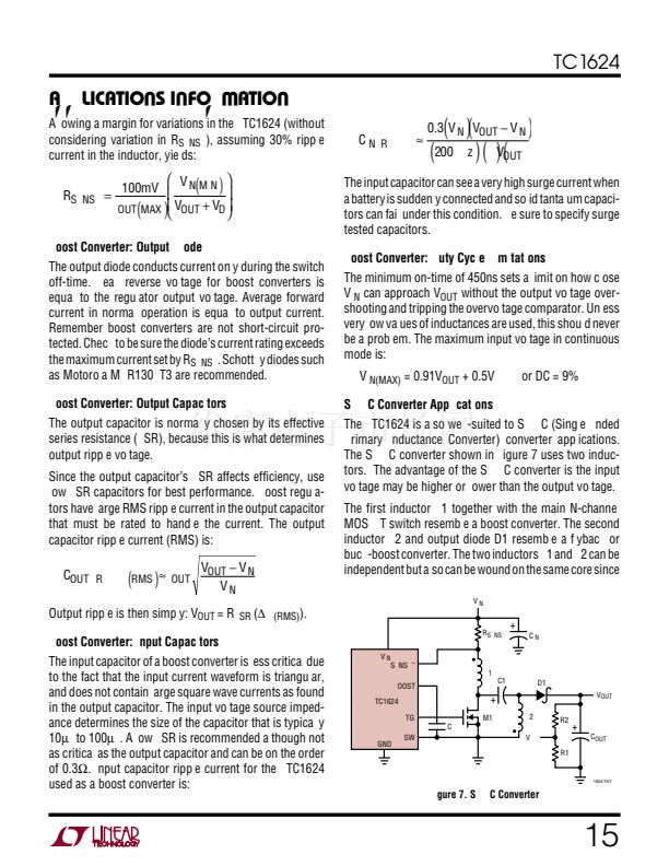
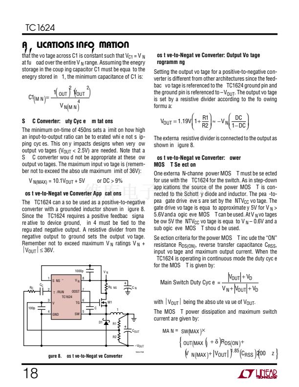
Boost Converter Applications
The LTC1624 is also well-suited to boost converter appli-
cations. A boost converter steps up the input voltage to a
higher voltage as shown in Figure 6.
V
IN
R
SENSE
+
C
IN
)
V
IN
SENSE
鈥?/div>
L1
BOOST
LTC1624
TG
C
B
GND
SW
V
FB
R1
M1
R2
D1
V
OUT
+
C
OUT
1624 F06
Figure 6. Boost Converter
13
LTC1624CS相关型号PDF文件下载
-
型号
版本
描述
厂商
下载
-
英文版
Dual Micropower Comparator
LINER
-
英文版
DUAL MICROPOWER COMPARATOR
LINER [Lin...
-
英文版
Dual Micropower Comparator
LINER [Lin...
-
英文版
BANG-BANG Controller
LINER
-
英文版
BANG-BANG Controller
LINER [Lin...
-
英文版
Window Comparator
LINER
-
英文版
Window Comparator
LINER [Lin...
-
英文版
Window Comparator
LINER [Lin...
-
英文版
2-Channel Differential Input 16-Bit No Latency DS ADC
LINER
-
英文版
2-Channel Differential Input 24-Bit No Latency DS ADC
LINER [Lin...
-
英文版
2-Channel Differential Input 16-Bit No Latency DS ADC
LINER [Lin...
-
英文版
Dual Precision Intrumentation Switched-Capacitor Building Bl...
LINER [Lin...
-
英文版
Switched Capacitor Voltage Converter
LINER
-
英文版
Switched Capacitor Voltage Converter
LINER [Lin...
-
英文版
Programmable Micropower Hex Translator/ Receiver/Driver
LINER
-
英文版
Programmable Micropower Hex Translator/ Receiver/Driver
LINER [Lin...
-
英文版
“Inductorless” 5V to + 5V Converter
LINER
-
英文版
“Inductorless” 5V to + 5V Converter
LINER [Lin...
-
英文版
Dual Micropower Chopper Stabilized Operational Amplifier wit...
LINER
-
英文版
Dual Micropower Zero-Drift Operational Amplifier with Intern...
LINER [Lin...


 1
1
 2
2
 3
3
 4
4
 5
5
 6
6
 7
7
 8
8
 9
9
 10
10
 11
11
 12
12
 13
13
 14
14
 15
15
 16
16
 17
17
 18
18
 19
19
 20
20
 21
21
 22
22
 23
23
 24
24
 25
25
 26
26
 27
27
 28
28
