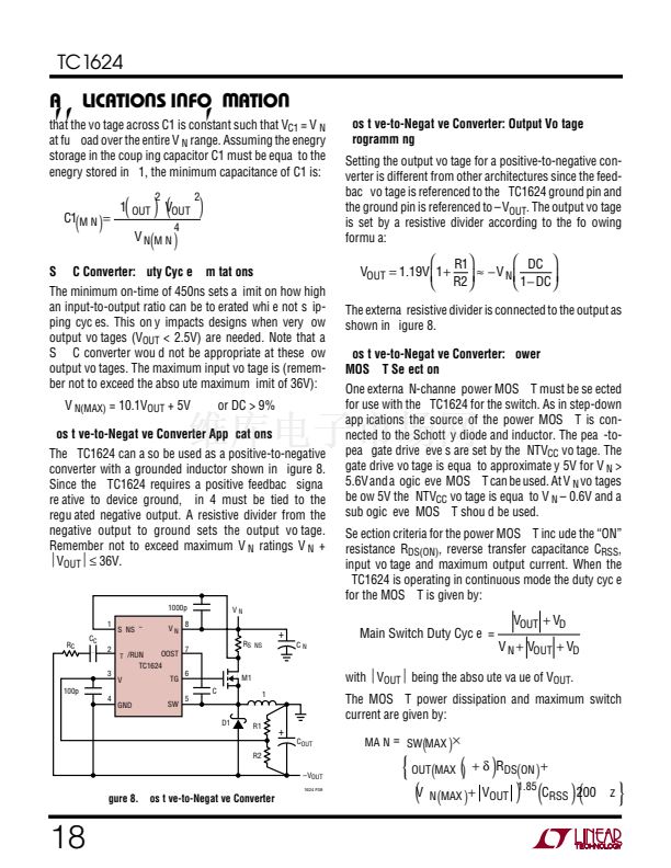
< 15V .................................. (V
鈮?/div>
15V .......................... (V
IN
+0.3V) to (V
IN
鈥?15V)
I
TH
/RUN, V
FB
Voltages ............................ 2.7V to 鈥?0.3V
Peak Driver Output Current < 10碌s (TG) .................... 2A
Operating Temperature Range
LTC1624CS ............................................ 0掳C to 70掳C
LTC1624IS ......................................... 鈥?40掳C to 85掳C
Junction Temperature (Note 1)............................. 125掳C
Storage Temperature Range ................. 鈥?65掳C to 150掳C
Lead Temperature (Soldering, 10 sec).................. 300掳C
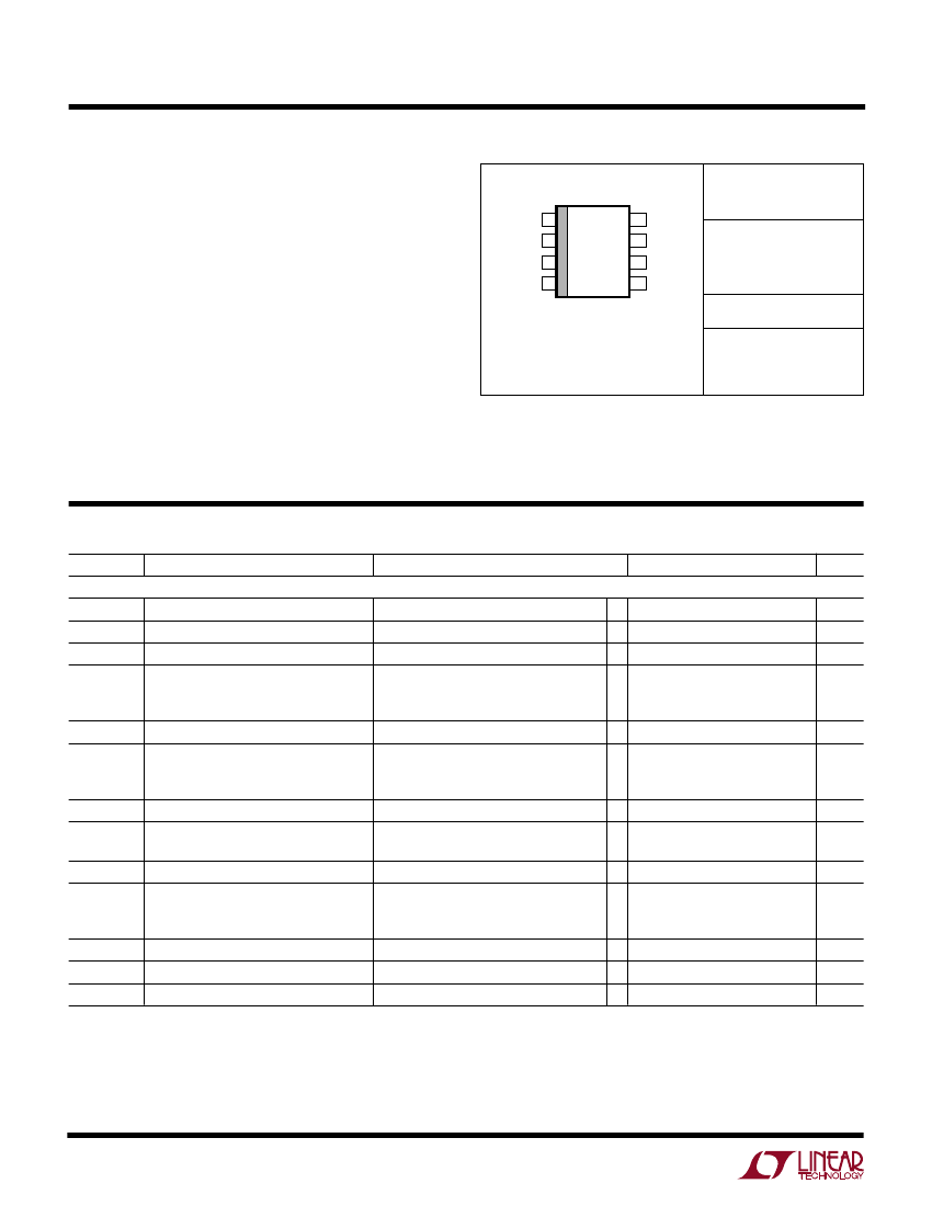
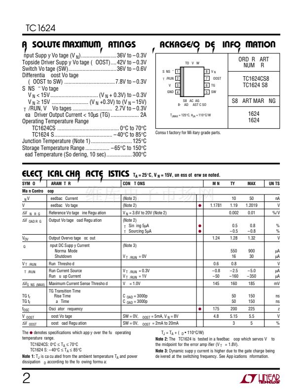
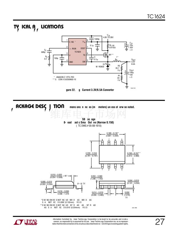
PACKAGE/ORDER INFORMATION
TOP VIEW
SENSE
鈥?/div>
1
I
TH
/RUN 2
V
FB
3
GND 4
8
7
6
5
V
IN
BOOST
TG
SW
ORDER PART
NUMBER
LTC1624CS8
LTC1624IS8
S8 PART MARKING
1624
1624I
S8 PACKAGE
8-LEAD PLASTIC SO
T
JMAX
= 125掳C,
胃
JA
= 110掳C/ W
Consult factory for Military grade parts.
ELECTRICAL CHARACTERISTICS
SYMBOL
I
IN
V
FB
V
FB
鈭哣
LINE REG
鈭哣
LOAD REG
PARAMETER
Feedback Current
Feedback Voltage
Reference Voltage Line Regulation
Output Voltage Load Regulation
Main Control Loop
T
A
= 25掳C, V
IN
= 15V, unless otherwise noted.
MIN
TYP
10
q
CONDITIONS
(Note 2)
(Note 2)
V
IN
= 3.6V to 20V (Note 2)
(Note 2)
I
TH
Sinking 5碌A
I
TH
Sourcing 5碌A
(Note 3)
V
ITH/RUN
= 0V
q
q
MAX
50
1.2019
0.01
0.8
鈥?0.8
1.32
900
30
鈥?5.0
鈥?350
185
150
150
225
5.5
5
UNITS
nA
V
%/V
%
%
V
碌A
碌A
V
碌A
碌A
mV
ns
ns
kHz
V
%
1.1781
1.19
0.002
0.5
鈥?0.5
V
OVL
I
Q
Output Overvoltage Lockout
Input DC Supply Current
Normal Mode
Shutdown
Run Threshold
Run Current Source
Run Pullup Current
TG Transition Time
Rise Time
Fall Time
Oscillator Frequency
Boost Voltage
Boost Load Regulation
SW = 0V, I
BOOST
= 5mA, V
IN
= 8V
SW = 0V, I
BOOST
= 2mA to 20mA
V
ITH/RUN
= 0.3V
V
ITH/RUN
= 1V
V
FB
= 1.0V
C
LOAD
= 3000pF
C
LOAD
= 3000pF
q
1.24
1.28
550
16
V
ITH/RUN
I
ITH/RUN
0.6
鈥?0.8
鈥?50
145
0.8
鈥?2.5
鈥?60
160
50
50
鈭哣
SENSE(MAX)
Maximum Current Sense Threshold
TG t
r
TG t
f
f
OSC
V
BOOST
鈭哣
BOOST
175
4.8
200
5.15
3
The
q
denotes specifications which apply over the full operating
temperature range.
LTC1624CS: 0掳C
鈮?/div>
T
A
鈮?/div>
70掳C
LTC1624IS: 鈥?40掳C
鈮?/div>
T
A
鈮?/div>
85掳C
Note 1:
T
J
is calculated from the ambient temperature T
A
and power
dissipation P
D
according to the following formula:
T
J
= T
A
+ (P
D
鈥?110掳C/W)
Note 2:
The LTC1624 is tested in a feedback loop which servos V
FB
to
the midpoint for the error amplifier (V
ITH
= 1.8V).
Note 3:
Dynamic supply current is higher due to the gate charge being
delivered at the switching frequency. See Applications Information.
2
U
W
U
U
W W
W
LTC1624CS相关型号PDF文件下载
-
型号
版本
描述
厂商
下载
-
英文版
Dual Micropower Comparator
LINER
-
英文版
DUAL MICROPOWER COMPARATOR
LINER [Lin...
-
英文版
Dual Micropower Comparator
LINER [Lin...
-
英文版
BANG-BANG Controller
LINER
-
英文版
BANG-BANG Controller
LINER [Lin...
-
英文版
Window Comparator
LINER
-
英文版
Window Comparator
LINER [Lin...
-
英文版
Window Comparator
LINER [Lin...
-
英文版
2-Channel Differential Input 16-Bit No Latency DS ADC
LINER
-
英文版
2-Channel Differential Input 24-Bit No Latency DS ADC
LINER [Lin...
-
英文版
2-Channel Differential Input 16-Bit No Latency DS ADC
LINER [Lin...
-
英文版
Dual Precision Intrumentation Switched-Capacitor Building Bl...
LINER [Lin...
-
英文版
Switched Capacitor Voltage Converter
LINER
-
英文版
Switched Capacitor Voltage Converter
LINER [Lin...
-
英文版
Programmable Micropower Hex Translator/ Receiver/Driver
LINER
-
英文版
Programmable Micropower Hex Translator/ Receiver/Driver
LINER [Lin...
-
英文版
“Inductorless” 5V to + 5V Converter
LINER
-
英文版
“Inductorless” 5V to + 5V Converter
LINER [Lin...
-
英文版
Dual Micropower Chopper Stabilized Operational Amplifier wit...
LINER
-
英文版
Dual Micropower Zero-Drift Operational Amplifier with Intern...
LINER [Lin...


 1
1
 2
2
 3
3
 4
4
 5
5
 6
6
 7
7
 8
8
 9
9
 10
10
 11
11
 12
12
 13
13
 14
14
 15
15
 16
16
 17
17
 18
18
 19
19
 20
20
 21
21
 22
22
 23
23
 24
24
 25
25
 26
26
 27
27
 28
28
