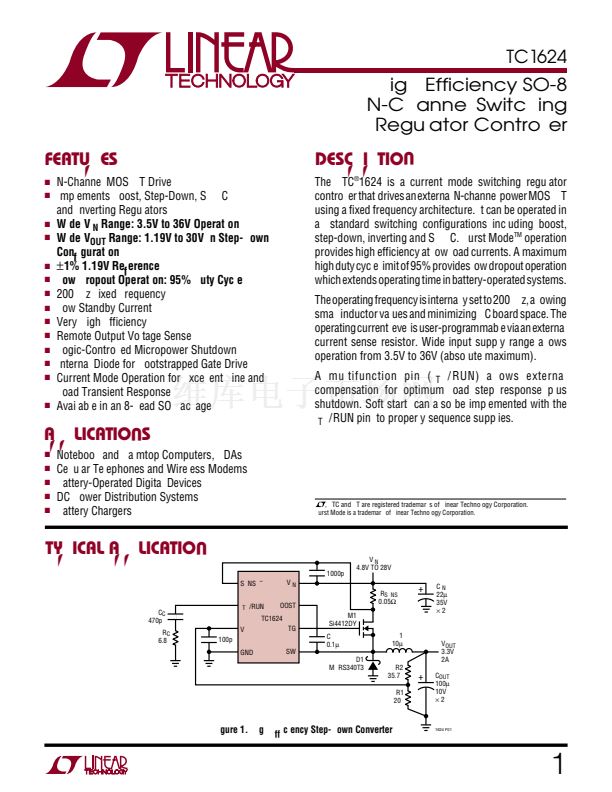
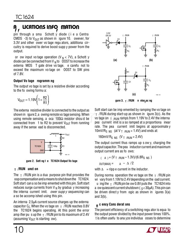
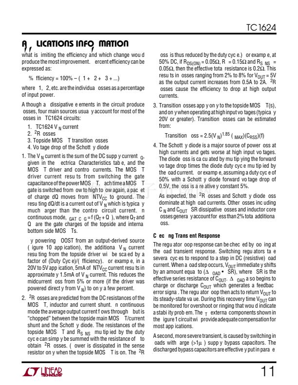
comparator. Built-in offsets between the SENSE
鈥?/div>
and V
IN
pins in conjunction with R
SENSE
set the current trip thresh-
olds. Do not pull this pin more than 15V below V
IN
or more
than 0.3V below ground.
I
TH
/RUN (Pin 2):
Combination of Error Amplifier Compen-
sation Point and Run Control Inputs. The current com-
parator threshold increases with this control voltage.
Nominal voltage range for this pin is 1.19V to 2.4V. Forcing
this pin below 0.8V causes the device to be shut down. In
shutdown all functions are disabled and TG pin is held low.
V
FB
(Pin 3):
Receives the feedback voltage from an exter-
nal resistive divider across the output.
GND (Pin 4):
Ground. Connect to the (鈥? terminal of C
OUT
,
the Schottky diode and the (鈥? terminal of C
IN
.
SW (Pin 5):
Switch Node Connection to Inductor. In step-
down applications the voltage swing at this pin is from a
Schottky diode (external) voltage drop below ground to
V
IN
.
4
U W
1624 G01
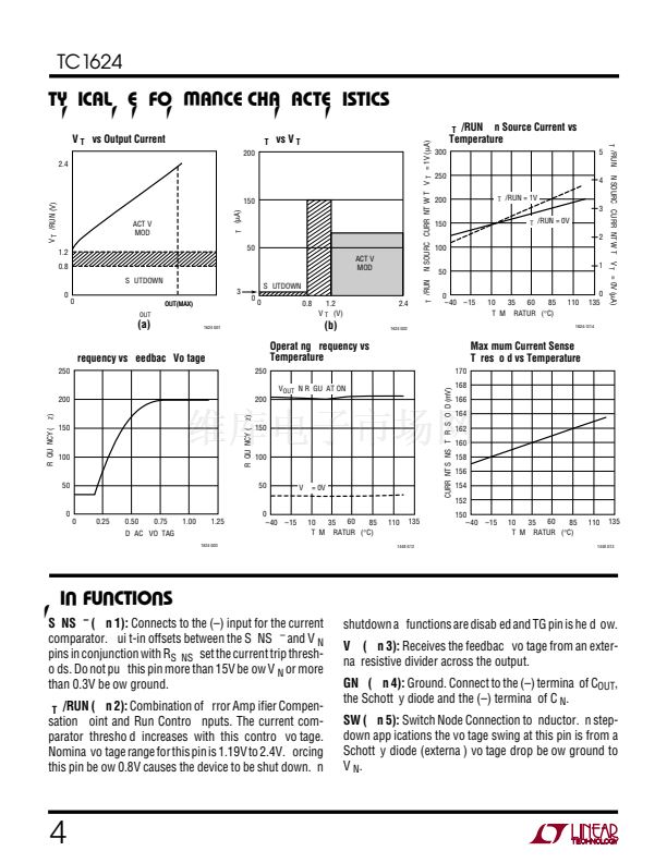
I
ITH
vs V
ITH
I
TH
/RUN Pin Source Current vs
Temperature
300
250
200
150
100
50
0
鈥?0 鈥?5
1
I
TH
/RUN = 1V
3
I
TH
/RUN = 0V
2
5
I
TH
/RUN PIN SOURCE CURRENT WITH V
ITH
= 0V (碌A)
4
150
50
ACTIVE
MODE
3
SHUTDOWN
0
0
0.8
1.2
V
ITH
(V)
2.4
60
35
85
10
TEMPERATURE (掳C)
110
0
135
(b)
1624 G02
1624 G14
Operating Frequency vs
Temperature
170
V
OUT
IN REGULATION
168
166
164
162
160
158
156
154
152
Maximum Current Sense
Threshold vs Temperature
150
100
50
V
FB
= 0V
0
鈥?0 鈥?5
60
10
85
35
TEMPERATURE (掳C)
110
135
150
鈥?0 鈥?5
60
35
10
85
TEMPERATURE (掳C)
110
135
1448 G12
1448 G13
U
U
U


 1
1
 2
2
 3
3
 4
4
 5
5
 6
6
 7
7
 8
8
 9
9
 10
10
 11
11
 12
12
 13
13
 14
14
 15
15
 16
16
 17
17
 18
18
 19
19
 20
20
 21
21
 22
22
 23
23
 24
24
 25
25
 26
26
 27
27
 28
28
