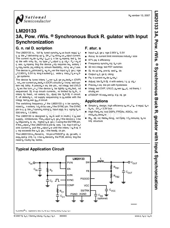
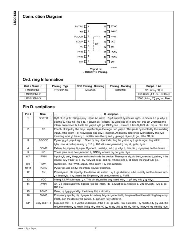
LM20133
Symbol
Enable
V
IH_EN
V
EN_HYS
T
SD
T
SD_HYS
胃
JA
Parameter
EN Pin Turn on Threshold
EN Pin Hysteresis
Thermal Shutdown
Thermal Shutdown Hysteresis
Junction to Ambient
Conditions
V
EN
Rising
Min
1.08
Typ
1.18
66
160
10
38
Max
1.28
Unit
V
mV
掳C
掳C
掳C/W
Thermal Shutdown
Thermal Resistance
Note 1:
Absolute Maximum Ratings indicate limits beyond which damage to the device may occur. Operating Ratings indicate conditions for which the device is
intended to be functional, but do not guarantee specific performance limits. For guaranteed specifications and test conditions, see the Electrical Characteristics.
Note 2:
The maximum allowable power dissipation is a function of the maximum junction temperature, T
J_MAX
, the junctions-to-ambient thermal resistance,
胃
JA
,
and the ambient temperature, T
A
. The maximum allowable power dissipation at any ambient temperature is calculated using: P
D_MAX
= (T
J_MAX
鈥?T
A
)/胃
JA
. The
maximum power dissipations of 2.6W is determined using T
A
= 25掳C,
胃
JA
= 38掳C/W, and T
J_MAX
= 125掳C.
Note 3:
The human body model is a 100 pF capacitor discharged through a 1.5 k鈩?resistor to each pin.
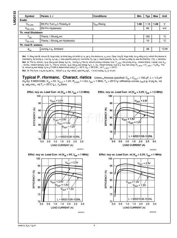
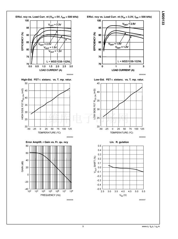
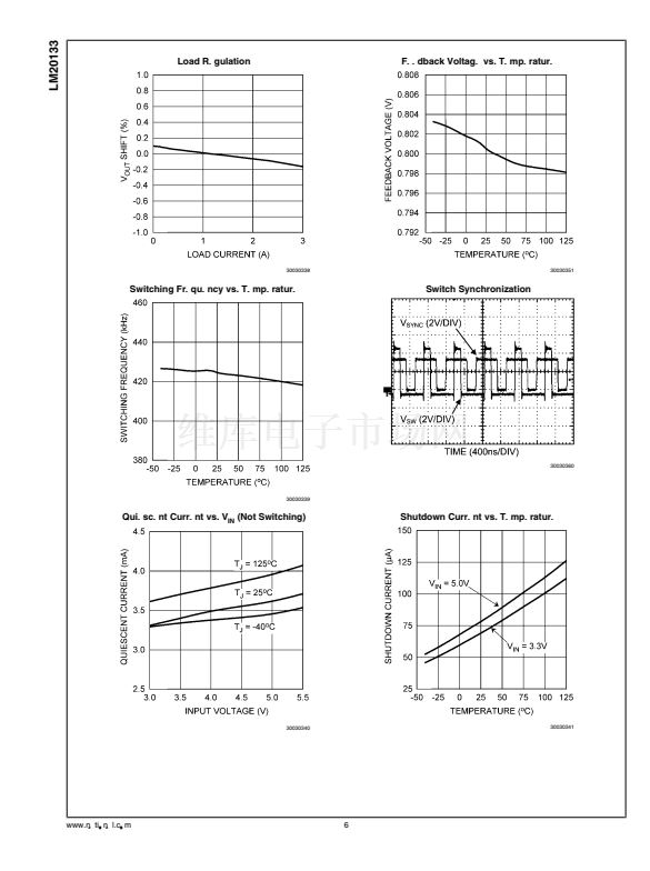
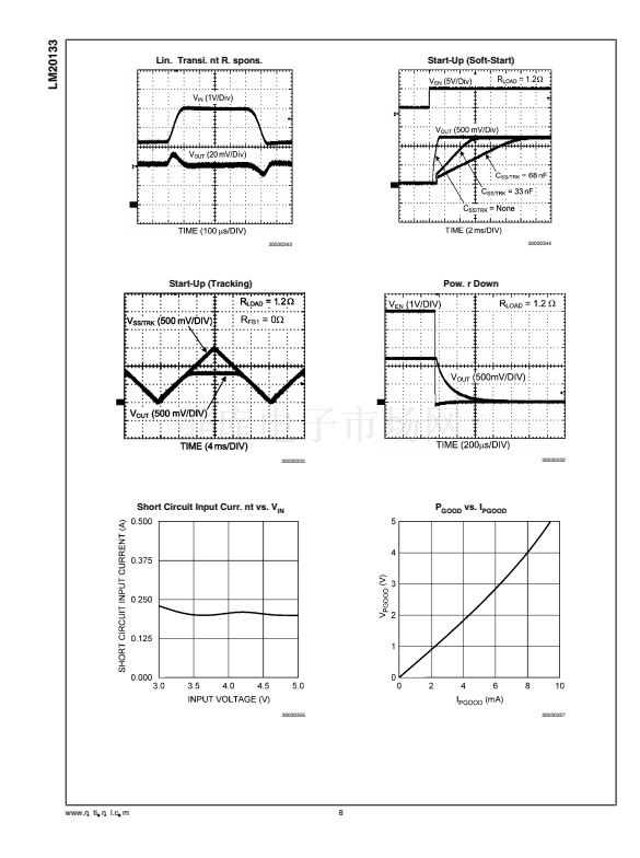
Typical Performance Characteristics
Unless otherwise specified: C
IN
= C
OUT
= 100 碌F, L = 1.0 碌H
(Coilcraft MSS1038), V
IN
= 5V, V
OUT
= 1.2V, R
LOAD
= 1.2鈩?
f
SW
= 1 MHz, T
A
= 25掳C for efficiency curves, loop gain plots and
waveforms, and T
J
= 25掳C for all others.
Efficiency vs. Load Current (V
IN
= 5V, f
SW
= 1.5 MHz)
Efficiency vs. Load Current (V
IN
= 3.3V, f
SW
= 1.5 MHz)
30030331
30030330
Efficiency vs. Load Current (V
IN
= 5V, f
SW
= 1 MHz)
Efficiency vs. Load Current (V
IN
= 3.3V, f
SW
= 1 MHz)
30030347
30030346
www.national.com
4


 1
1
 2
2
 3
3
 4
4
 5
5
 6
6
 7
7
 8
8
 9
9
 10
10
 11
11
 12
12
 13
13
 14
14
 15
15
 16
16
 17
17
 18
18
 19
19
 20
20
 21
21
 22
22
