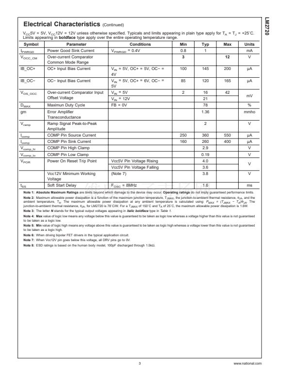
IB_OC鈭?/div>
V
OS_OCC
D
MAX
gm
V
ramp
I
comp
I
comp
V
comp_hi
V
comp_lo
V
POR
Parameter
Power Good Sink Current
Over-current Comparator
Common Mode Range
OC+ Input Bias Current
OC鈭?Input Bias Current
(Continued)
V
CC
5V = 5V, V
CC
12V = 12V unless otherwise specified. Typicals and limits appearing in plain type apply for T
A
= T
J
= +25藲C.
Limits appearing in
boldface
type apply over the entire operating temperature range.
V
PWRGD
Conditions
= 0.4V
Min
0.8
3
V
IN
= 5V, OC+ = 5V, OC鈭?=
4V
V
IN
= 5V, OC+ = 6V, OC鈭?=
5V
V
IN
= 5V
V
IN
= 12V
FB = 0V
100
85
2
145
120
16
21
78
1.36
2
250
160
360
260
2.9
0.19
Vcc5V Pin Voltage Rising
Vcc5V Pin Voltage Falling
Vcc12V Minimum Working
Voltage
t
SS
Soft Start Delay
(Note 7)
F
OSC
= 8MHz
4.0
3.6
3.8
1.6
550
400
Typ
1
12
200
165
42
Max
Units
mA
V
碌A
碌A
Over-current Comparator Input
Offset Voltage
Maximun Duty Cycle
Error Amplifier
Transconductance
Ramp Signal Peak-to-Peak
Amplitude
COMP Pin Source Current
COMP Pin Sink Current
COMP Pin High Clamp
COMP Pin Low Clamp
Power On Reset Trip Point
mV
%
mmho
V
碌A
碌A
V
V
V
V
ms
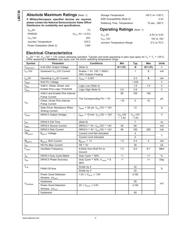
Note 1: Absolute Maximum Ratings
are limits beyond which damage to the device may occur.
Operating ratings
do not imply guaranteed performance limits.
Note 2:
Maximum allowable power dissipation is a function of the maximum junction temperature, T
JMAX
, the junction-to-ambient thermal resistance,
胃
JA
, and the
ambient temperature, T
A
. The maximum allowable power dissipation at any ambient temperature is calculated using:
P
MAX
= (T
JMAX
鈭?T
A
)/
胃
JA
.
The
junction-to-ambient thermal resistance,
胃
JA
, for LM2720 is 78藲C/W. For a T
JMAX
of 150藲C and T
A
of 25藲C, the maximum allowable power dissipation is 1.6W.
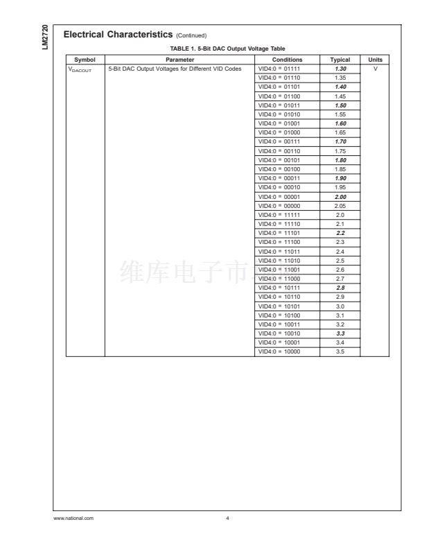
Note 3:
The letter
N
stands for the typical output voltages appearing in
italic boldface
type in
Table 1.
Note 4: Max
value of logic low means any voltage below this value is guaranteed to be taken as logic low whereas a voltage higher than this value is not guaranteed
to be taken as a logic low.
Note 5: Min
value of logic high means any voltage above this value is guaranteed to be taken as logic high whereas a voltage lower than this value is not guaranteed
to be taken as a logic high.
Note 6:
When driving bipolar FET drivers in the typical application circuit.
Note 7:
When Vcc12V pin goes below this voltage, all DRV pins go to 0V.
Note 8:
ESD ratings is based on the human body model, 100pF discharged through 1.5k鈩?
3
www.national.com


 1
1
 2
2
 3
3
 4
4
 5
5
 6
6
 7
7
 8
8
