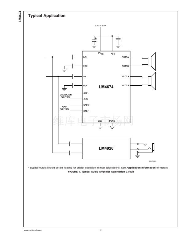
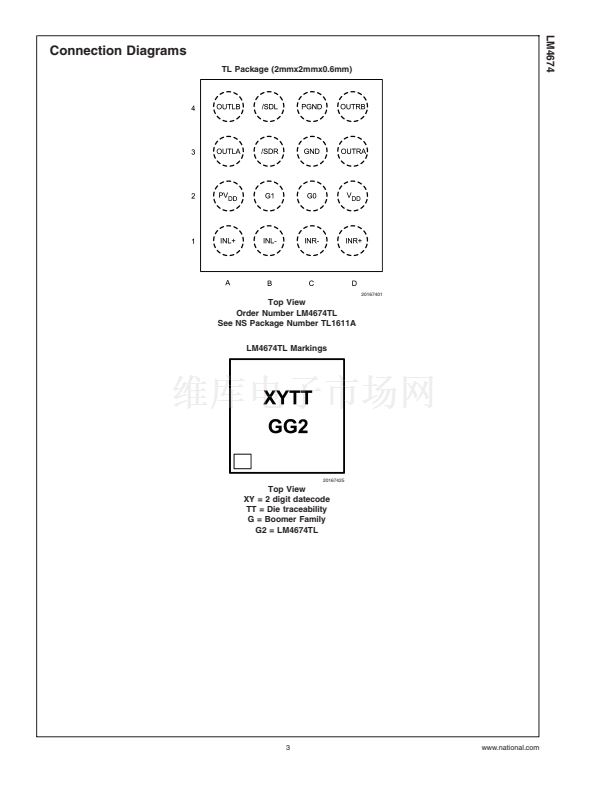
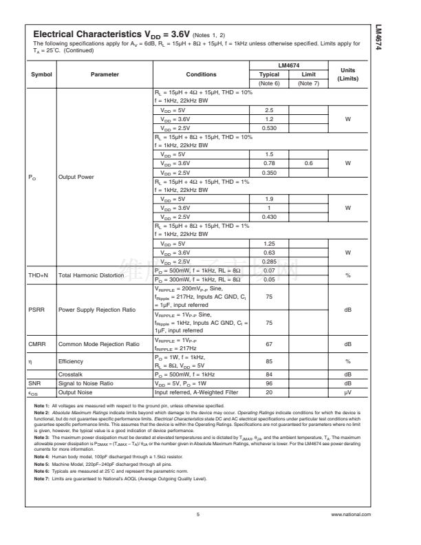
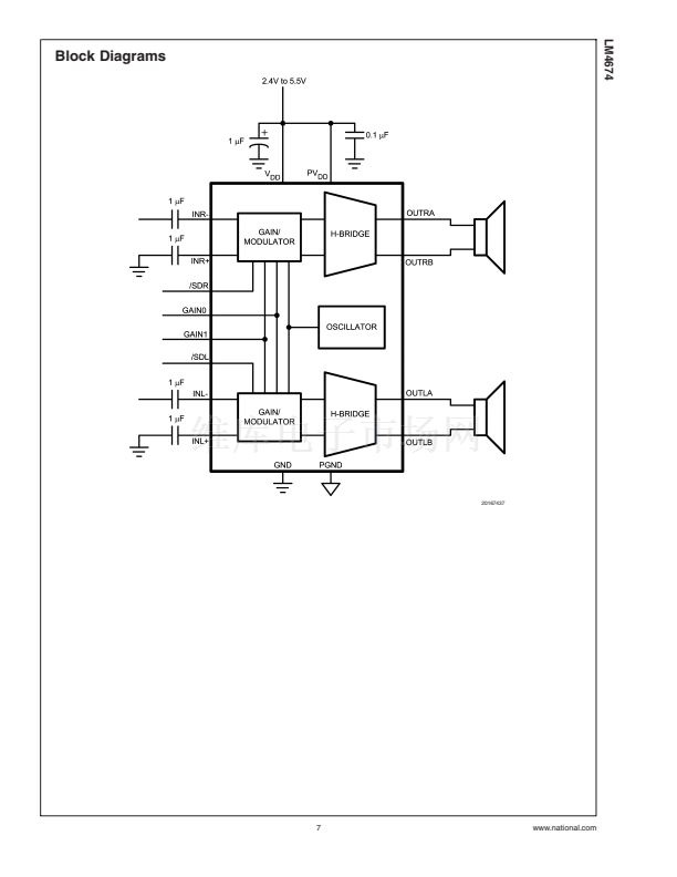
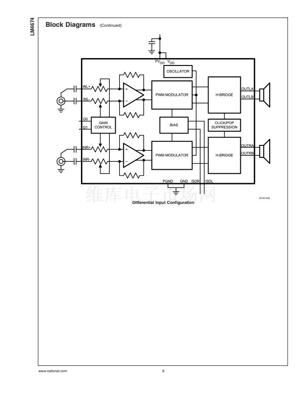
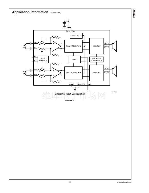
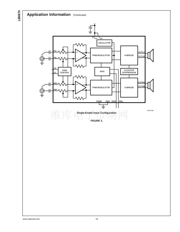
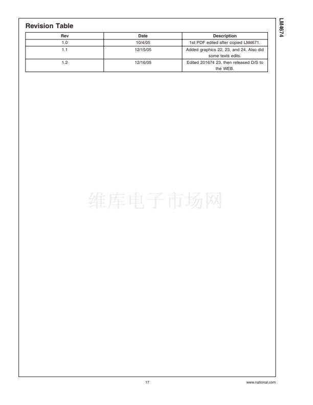
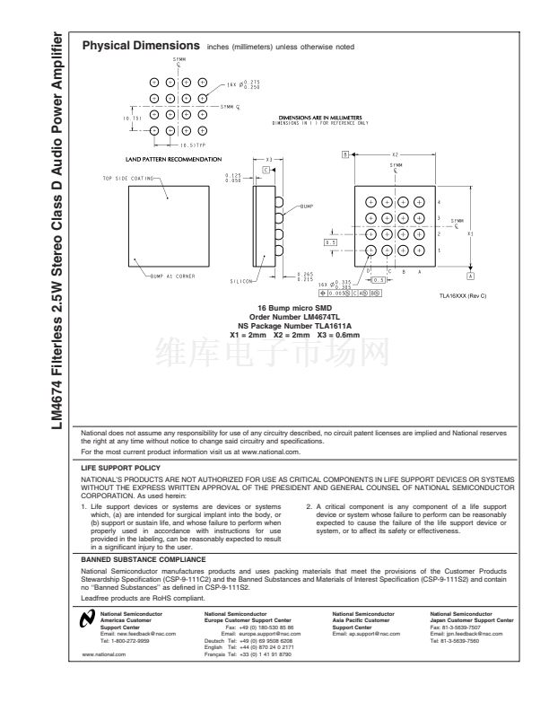
LM4674
Application Information
PCB LAYOUT GUIDELINES
(Continued)
As output power increases, interconnect resistance (PCB
traces and wires) between the amplifier, load and power
supply create a voltage drop. The voltage loss due to the
traces between the LM4674 and the load results in lower
output power and decreased efficiency. Higher trace resis-
tance between the supply and the LM4674 has the same
effect as a poorly regulated supply, increasing ripple on the
supply line, and reducing peak output power. The effects of
residual trace resistance increases as output current in-
creases due to higher output power, decreased load imped-
ance or both. To maintain the highest output voltage swing
and corresponding peak output power, the PCB traces that
connect the output pins to the load and the supply pins to the
power supply should be as wide as possible to minimize
trace resistance.
The use of power and ground planes will give the best
THD+N performance. In addition to reducing trace resis-
tance, the use of power planes creates parasitic capacitors
that help to filter the power supply line.
The inductive nature of the transducer load can also result in
overshoot on one of both edges, clamped by the parasitic
diodes to GND and VDD in each case. From an EMI stand-
point, this is an aggressive waveform that can radiate or
conduct to other components in the system and cause inter-
ference. In is essential to keep the power and output traces
short and well shielded if possible. Use of ground planes
beads and micros-strip layout techniques are all useful in
preventing unwanted interference.
As the distance from the LM4674 and the speaker increases,
the amount of EMI radiation increases due to the output
wires or traces acting as antennas become more efficient
with length. Ferrite chip inductors places close to the
LM4674 outputs may be needed to reduce EMI radiation.
www.national.com
14


 1
1
 2
2
 3
3
 4
4
 5
5
 6
6
 7
7
 8
8
 9
9
 10
10
 11
11
 12
12
 13
13
 14
14
 15
15
 16
16
 17
17
 18
18
