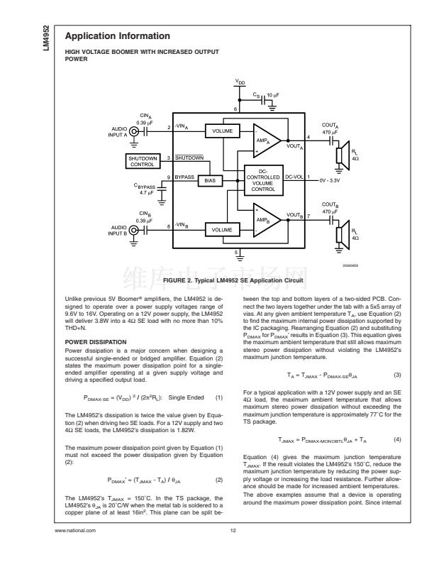
LM4952
Application Information
(Continued)
manner, the ground lead of the capacitor connected between
the BYPASS pin and GND should also be connected to the
package鈥檚 grounded tab.
OPTIMIZING CLICK AND POP REDUCTION
PERFORMANCE
The LM4952 contains circuitry that eliminates turn-on and
shutdown transients ("clicks and pops"). For this discussion,
turn-on refers to either applying the power supply voltage or
when the micro-power shutdown mode is deactivated.
As the V
DD
/4 voltage present at the BYPASS pin ramps to its
final value, the LM4952鈥檚 internal amplifiers are muted. Once
the voltage at the BYPASS pin reaches V
DD
/4, the amplifiers
are unmuted.
The gain of the internal amplifiers remains unity until the
voltage on the bypass pin reaches V
DD
/4. As soon as the
voltage on the bypass pin is stable, the device becomes fully
operational and the amplifier outputs are reconnected to
their respective output pins.
In order eliminate "clicks and pops", all capacitors must be
discharged before turn-on. Rapidly switching V
DD
may not
allow the capacitors to fully discharge, which may cause
"clicks and pops".
There is a relationship between the value of C
IN
and
C
BYPASS
that ensures minimum output transient when power
is applied or the shutdown mode is deactivated. Best perfor-
mance is achieved by selecting a C
BYPASS
value that is
greater than twelve times C
IN
鈥檚 value.
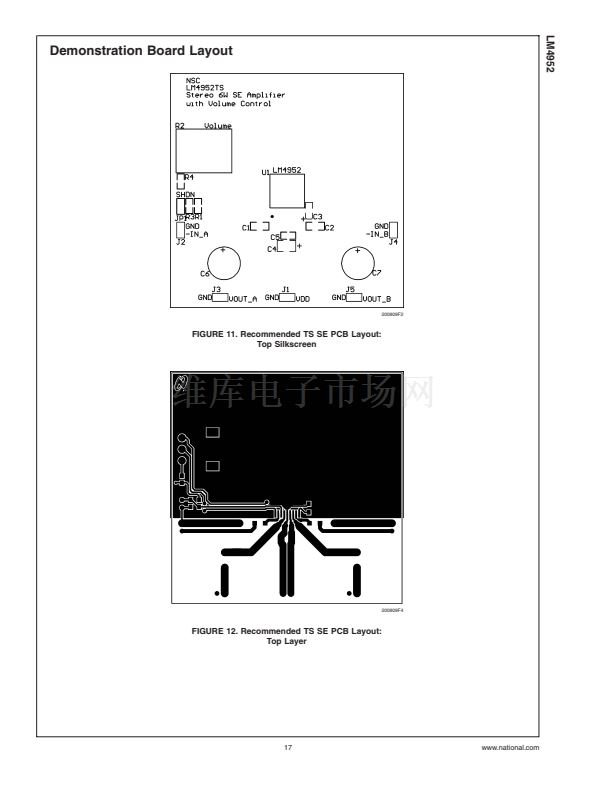
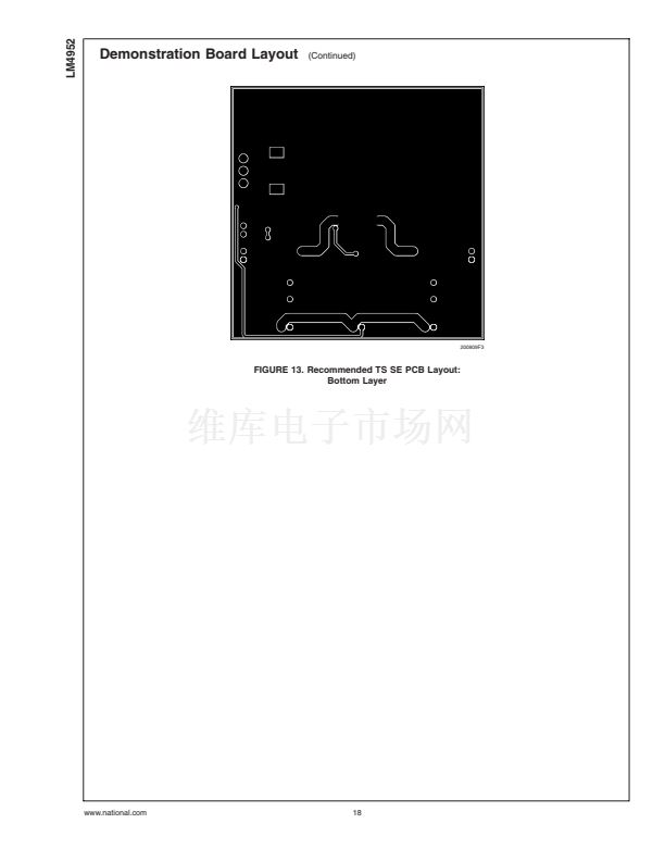
RECOMMENDED PRINTED CIRCUIT BOARD LAYOUT
Figure 9 through Figure 11 show the recommended two-
layer PC board layout that is optimized for the TO263-
packaged, SE-configured LM4952 and associated external
components. These circuits are designed for use with an
external 12V supply and 4鈩?min)(SE) speakers.
These circuit boards are easy to use. Apply 12V and ground
to the board鈥檚 V
DD
and GND pads, respectively. Connect a
speaker between the board鈥檚 OUT
A
and OUT
B
outputs and
respective GND pins.
www.national.com
16


 1
1
 2
2
 3
3
 4
4
 5
5
 6
6
 7
7
 8
8
 9
9
 10
10
 11
11
 12
12
 13
13
 14
14
 15
15
 16
16
 17
17
 18
18
 19
19
 20
20
