LM4952
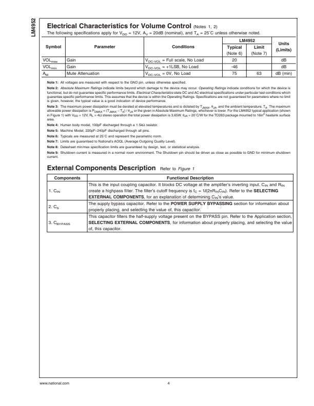
Electrical Characteristics for Volume Control
(Notes 1, 2)
The following specifications apply for V
DD
= 12V, A
V
= 20dB (nominal), and T
A
= 25藲C unless otherwise noted.
LM4952
Symbol
VOL
max
VOL
min
A
M
Gain
Gain
Mute Attenuation
Parameter
Conditions
V
DC-VOL
= Full scale, No Load
V
DC-VOL
= +1LSB, No Load
V
DC-VOL
= 0V, No Load
Typical
(Note 6)
20
-46
75
63
Limit
(Note 7)
Units
(Limits)
dB
dB
dB (min)
Note 1:
All voltages are measured with respect to the GND pin, unless otherwise specified.
Note 2:
Absolute Maximum Ratings
indicate limits beyond which damage to the device may occur.
Operating Ratings
indicate conditions for which the device is
functional, but do not guarantee specific performance limits.
Electrical Characteristics
state DC and AC electrical specifications under particular test conditions which
guarantee specific performance limits. This assumes that the device is within the Operating Ratings. Specifications are not guaranteed for parameters where no limit
is given, however, the typical value is a good indication of device performance.
Note 3:
The maximum power dissipation must be derated at elevated temperatures and is dictated by T
JMAX
,
胃
JA
, and the ambient temperature, T
A
. The maximum
allowable power dissipation is P
DMAX
= (T
JMAX
鈭?T
A
) /
胃
JA
or the given in Absolute Maximum Ratings, whichever is lower. For the LM4952 typical application (shown
in Figure 1) with V
DD
= 12V, R
L
= 4鈩?stereo operation the total power dissipation is 3.65W.
胃
JA
= 20藲C/W for the TO263 package mounted to 16in
2
heatsink surface
area.
Note 4:
Human body model, 100pF discharged through a 1.5k鈩?resistor.
Note 5:
Machine Model, 220pF鈥?40pF discharged through all pins.
Note 6:
Typicals are measured at 25藲C and represent the parametric norm.
Note 7:
Limits are guaranteed to National鈥檚 AOQL (Average Outgoing Quality Level).
Note 8:
Datasheet min/max specification limits are guaranteed by design, test, or statistical analysis.
Note 9:
Shutdown current is measured in a normal room environment. The Shutdown pin should be driven as close as possible to GND for minimum shutdown
current.
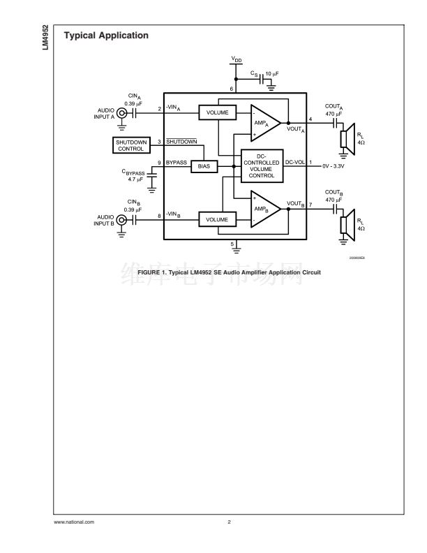
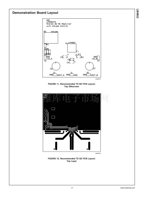
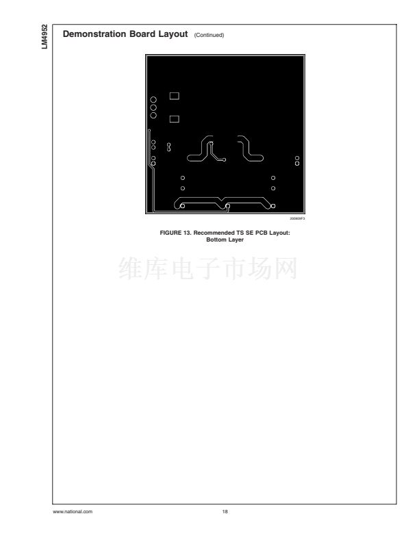
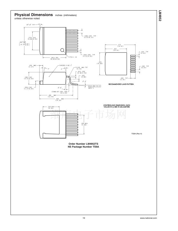
External Components Description
Components
1. C
IN
Refer to
Figure 1
Functional Description
This is the input coupling capacitor. It blocks DC voltage at the amplifier鈥檚 inverting input. C
IN
and R
IN
create a highpass filter. The filter鈥檚 cutoff frequency is f
C
= 1/(2蟺R
IN
C
IN
). Refer to the
SELECTING
EXTERNAL COMPONENTS,
for an explanation of determining C
IN
鈥檚 value.
The supply bypass capacitor. Refer to the
POWER SUPPLY BYPASSING
section for information about
properly placing, and selecting the value of, this capacitor.
This capacitor filters the half-supply voltage present on the BYPASS pin. Refer to the Application section,
SELECTING EXTERNAL COMPONENTS,
for information about properly placing, and selecting the value
of, this capacitor.
2. C
S
3. C
BYPASS
www.national.com
4


 1
1
 2
2
 3
3
 4
4
 5
5
 6
6
 7
7
 8
8
 9
9
 10
10
 11
11
 12
12
 13
13
 14
14
 15
15
 16
16
 17
17
 18
18
 19
19
 20
20
