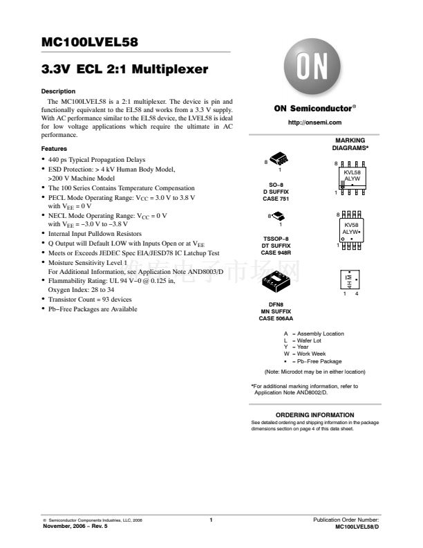
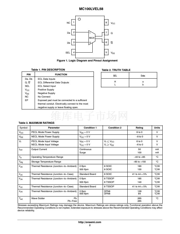
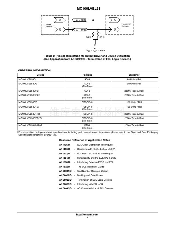
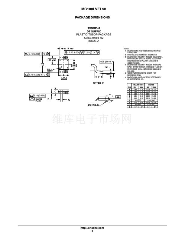
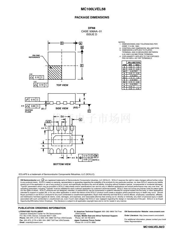
MC100LVEL58
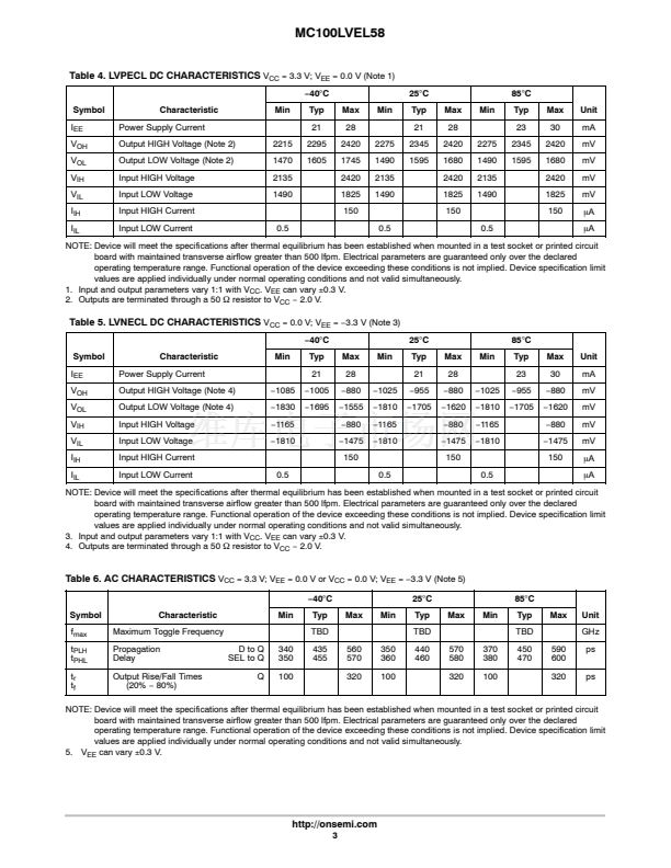
Table 4. LVPECL DC CHARACTERISTICS
V
CC
= 3.3 V; V
EE
= 0.0 V (Note 1)
鈭?0掳C
Symbol
I
EE
V
OH
V
OL
V
IH
V
IL
I
IH
I
IL
Characteristic
Power Supply Current
Output HIGH Voltage (Note 2)
Output LOW Voltage (Note 2)
Input HIGH Voltage
Input LOW Voltage
Input HIGH Current
Input LOW Current
0.5
2215
1470
2135
1490
Min
Typ
21
2295
1605
Max
28
2420
1745
2420
1825
150
0.5
2275
1490
2135
1490
Min
25掳C
Typ
21
2345
1595
Max
28
2420
1680
2420
1825
150
0.5
2275
1490
2135
1490
Min
85掳C
Typ
23
2345
1595
Max
30
2420
1680
2420
1825
150
Unit
mA
mV
mV
mV
mV
mA
mA
NOTE: Device will meet the specifications after thermal equilibrium has been established when mounted in a test socket or printed circuit
board with maintained transverse airflow greater than 500 lfpm. Electrical parameters are guaranteed only over the declared
operating temperature range. Functional operation of the device exceeding these conditions is not implied. Device specification limit
values are applied individually under normal operating conditions and not valid simultaneously.
1. Input and output parameters vary 1:1 with V
CC
. V
EE
can vary
卤0.3
V.
2. Outputs are terminated through a 50
W
resistor to V
CC
鈭?/div>
2.0 V.
Table 5. LVNECL DC CHARACTERISTICS
V
CC
= 0.0 V; V
EE
=
鈭?.3
V (Note 3)
鈭?0掳C
Symbol
I
EE
V
OH
V
OL
V
IH
V
IL
I
IH
I
IL
Characteristic
Power Supply Current
Output HIGH Voltage (Note 4)
Output LOW Voltage (Note 4)
Input HIGH Voltage
Input LOW Voltage
Input HIGH Current
Input LOW Current
0.5
鈭?085
鈭?830
鈭?165
鈭?810
Min
Typ
21
鈭?005
鈭?695
Max
28
鈭?80
鈭?555
鈭?80
鈭?475
150
0.5
鈭?025
鈭?810
鈭?165
鈭?810
Min
25掳C
Typ
21
鈭?55
鈭?705
Max
28
鈭?80
鈭?620
鈭?80
鈭?475
150
0.5
鈭?025
鈭?810
鈭?165
鈭?810
Min
85掳C
Typ
23
鈭?55
鈭?705
Max
30
鈭?80
鈭?620
鈭?80
鈭?475
150
Unit
mA
mV
mV
mV
mV
mA
mA
NOTE: Device will meet the specifications after thermal equilibrium has been established when mounted in a test socket or printed circuit
board with maintained transverse airflow greater than 500 lfpm. Electrical parameters are guaranteed only over the declared
operating temperature range. Functional operation of the device exceeding these conditions is not implied. Device specification limit
values are applied individually under normal operating conditions and not valid simultaneously.
3. Input and output parameters vary 1:1 with V
CC
. V
EE
can vary
卤0.3
V.
4. Outputs are terminated through a 50
W
resistor to V
CC
鈭?/div>
2.0 V.
Table 6. AC CHARACTERISTICS
V
CC
= 3.3 V; V
EE
= 0.0 V or V
CC
= 0.0 V; V
EE
=
鈭?.3
V (Note 5)
鈭?0掳C
Symbol
f
max
t
PLH
t
PHL
t
r
t
f
Characteristic
Maximum Toggle Frequency
Propagation
Delay
Output Rise/Fall Times
(20%
鈭?/div>
80%)
D to Q
SEL to Q
Q
340
350
100
Min
Typ
TBD
435
455
560
570
320
350
360
100
Max
Min
25掳C
Typ
TBD
440
460
570
580
320
370
380
100
Max
Min
85掳C
Typ
TBD
450
470
590
600
320
Max
Unit
GHz
ps
ps
NOTE: Device will meet the specifications after thermal equilibrium has been established when mounted in a test socket or printed circuit
board with maintained transverse airflow greater than 500 lfpm. Electrical parameters are guaranteed only over the declared
operating temperature range. Functional operation of the device exceeding these conditions is not implied. Device specification limit
values are applied individually under normal operating conditions and not valid simultaneously.
5. V
EE
can vary
卤0.3
V.
http://onsemi.com
3


 1
1
 2
2
 3
3
 4
4
 5
5
 6
6
 7
7
