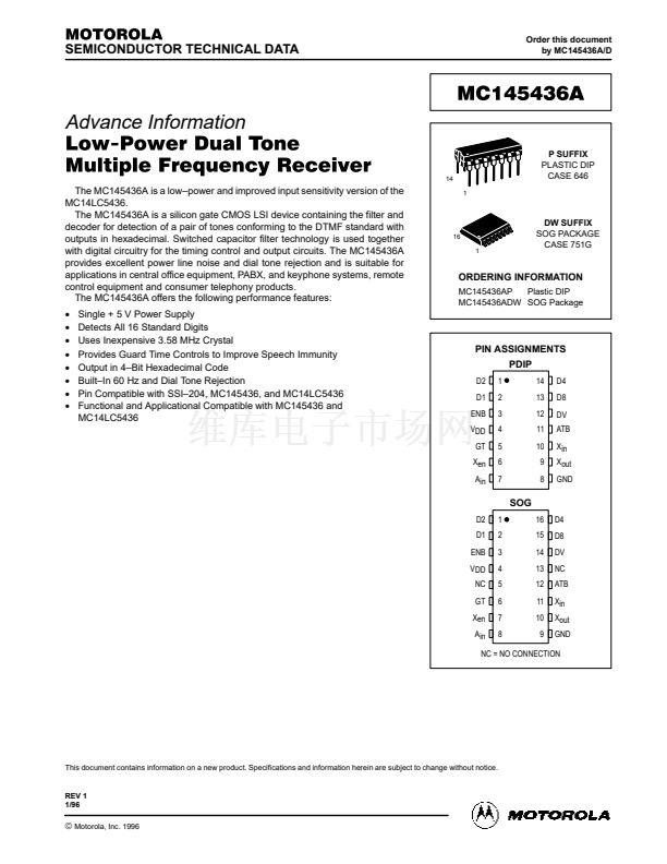
PIN DESCRIPTIONS
VDD
Positive Power Supply (PDIP, SOG 鈥?Pin 4)
The digital supply pin, which is connected to the positive
side of the power supply.
VSS
Ground (PDIP 鈥?Pin 8, SOG 鈥?Pin 9)
Ground return pin is typically connected to the system
ground.
D1, D2, D4, D8
Data Output (PDIP 鈥?Pins 2, 1, 14, 13; SOG 鈥?Pins 2, 1,
16, 15)
These digital outputs provide the hexadecimal codes cor-
responding to the detected digit. The digital outputs become
valid after a tone pair has been detected and are cleared
when a valid pause is timed. See Table 1 for hexadecimal
codes.These output pins are high impedance when the
enable pin is at logic 0.
ENB
Enable (PDIP, SOG 鈥?Pin 3)
Outputs D1, D2, D4, D8 are enabled when ENB is at a
logic 1, and high impedance (disabled) when ENB is at a
logic 0.
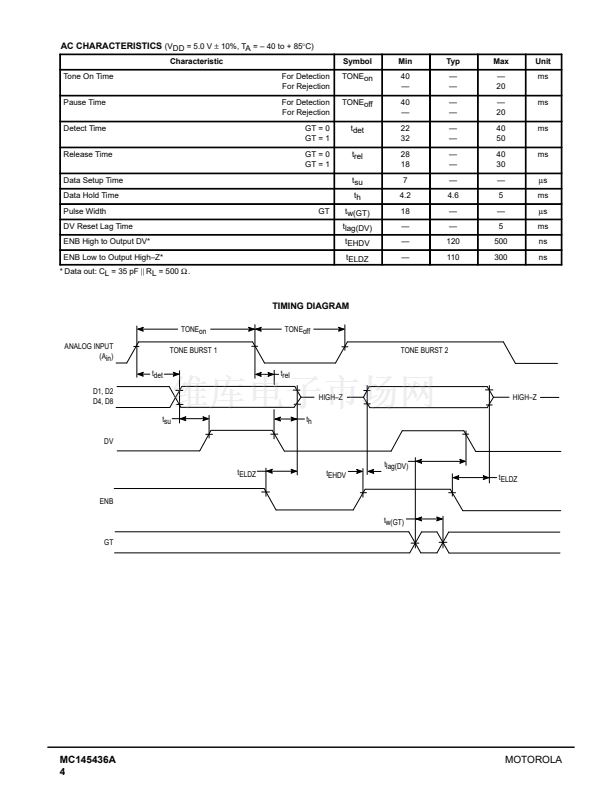
GT
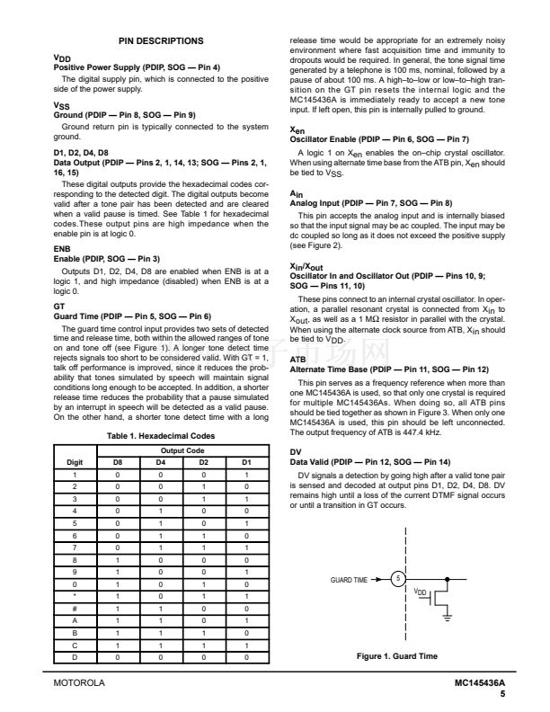
Guard Time (PDIP 鈥?Pin 5, SOG 鈥?Pin 6)
The guard time control input provides two sets of detected
time and release time, both within the allowed ranges of tone
on and tone off (see Figure 1). A longer tone detect time
rejects signals too short to be considered valid. With GT = 1,
talk off performance is improved, since it reduces the prob-
ability that tones simulated by speech will maintain signal
conditions long enough to be accepted. In addition, a shorter
release time reduces the probability that a pause simulated
by an interrupt in speech will be detected as a valid pause.
On the other hand, a shorter tone detect time with a long
Table 1. Hexadecimal Codes
Output Code
Digit
1
2
3
4
5
6
7
8
9
0
*
#
A
B
C
D
D8
0
0
0
0
0
0
0
1
1
1
1
1
1
1
1
0
D4
0
0
0
1
1
1
1
0
0
0
0
1
1
1
1
0
D2
0
1
1
0
0
1
1
0
0
1
1
0
0
1
1
0
D1
1
0
1
0
1
0
1
0
1
0
1
0
1
0
1
0
release time would be appropriate for an extremely noisy
environment where fast acquisition time and immunity to
dropouts would be required. In general, the tone signal time
generated by a telephone is 100 ms, nominal, followed by a
pause of about 100 ms. A high鈥搕o鈥搇ow or low鈥搕o鈥揾igh tran-
sition on the GT pin resets the internal logic and the
MC145436A is immediately ready to accept a new tone
input. If left open, this pin is internally pulled to ground.
Xen
Oscillator Enable (PDIP 鈥?Pin 6, SOG 鈥?Pin 7)
A logic 1 on Xen enables the on鈥揷hip crystal oscillator.
When using alternate time base from the ATB pin, Xen should
be tied to VSS.
Ain
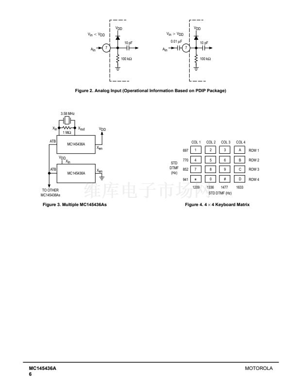
Analog Input (PDIP 鈥?Pin 7, SOG 鈥?Pin 8)
This pin accepts the analog input and is internally biased
so that the input signal may be ac coupled. The input may be
dc coupled so long as it does not exceed the positive supply
(see Figure 2).
Xin/Xout
Oscillator In and Oscillator Out (PDIP 鈥?Pins 10, 9;
SOG 鈥?Pins 11, 10)
These pins connect to an internal crystal oscillator. In oper-
ation, a parallel resonant crystal is connected from X in to
X out, as well as a 1 M
鈩?/div>
resistor in parallel with the crystal.
When using the alternate clock source from ATB, X in should
be tied to VDD.
ATB
Alternate Time Base (PDIP 鈥?Pin 11, SOG 鈥?Pin 12)
This pin serves as a frequency reference when more than
one MC145436A is used, so that only one crystal is required
for multiple MC145436As. When doing so, all ATB pins
should be tied together as shown in Figure 3. When only one
MC145436A is used, this pin should be left unconnected.
The output frequency of ATB is 447.4 kHz.
DV
Data Valid (PDIP 鈥?Pin 12, SOG 鈥?Pin 14)
DV signals a detection by going high after a valid tone pair
is sensed and decoded at output pins D1, D2, D4, D8. DV
remains high until a loss of the current DTMF signal occurs
or until a transition in GT occurs.
GUARD TIME
5
VDD
Figure 1. Guard Time
MOTOROLA
MC145436A
5


 1
1
 2
2
 3
3
 4
4
 5
5
 6
6
 7
7
 8
8
