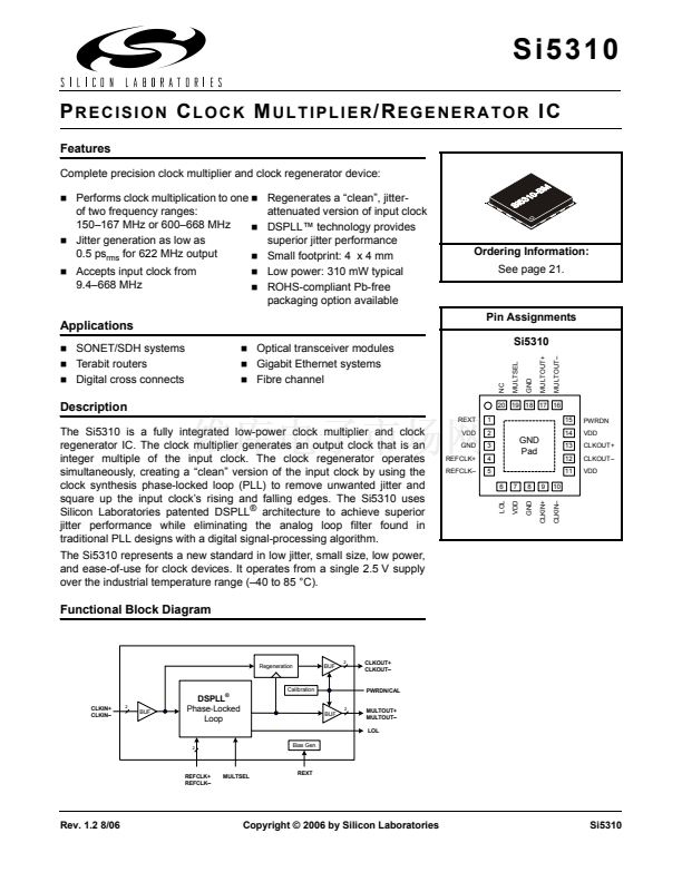
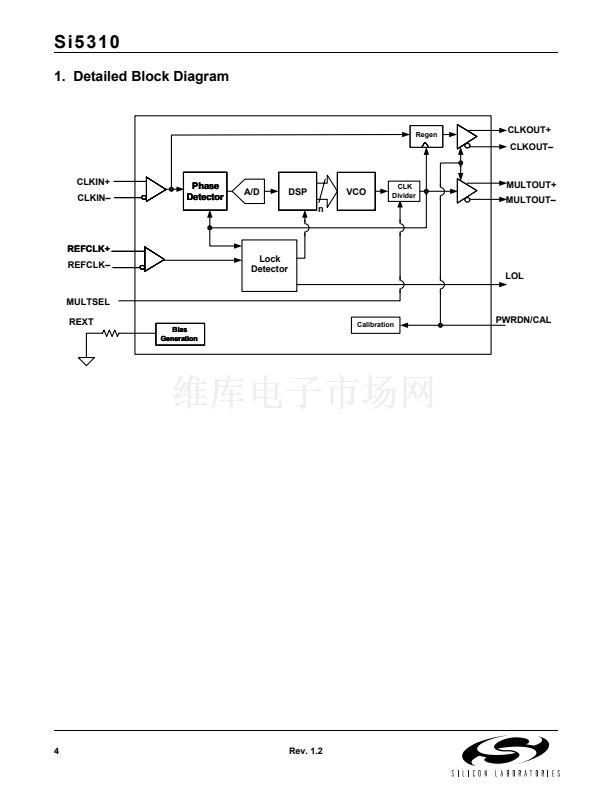
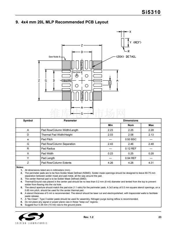
Si5310
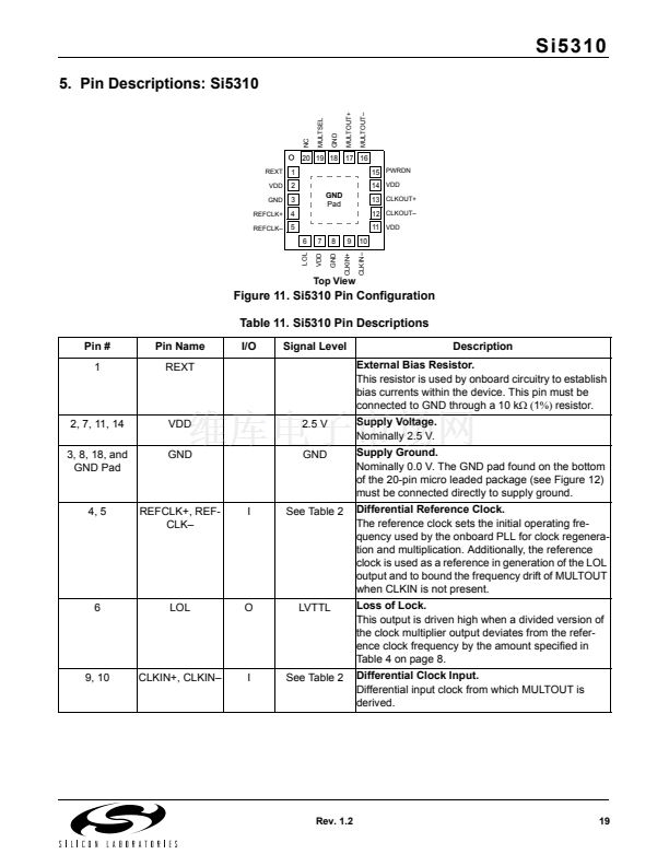
4.11. Bias Generation Circuitry
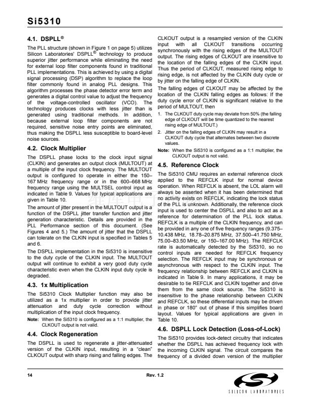
The Si5310 makes use of an external resistor to set
internal bias currents. The external resistor allows
precise generation of bias currents which significantly
reduces power consumption compared with traditional
implementations that use an internal resistor. The bias
generation circuitry requires a 10 k鈩?(1%) resistor
connected between REXT and GND.
0
CLKIN=622MHz
鈭?
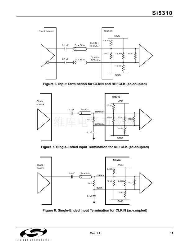
coupling is possible, the 0.1
碌F
capacitors may be
omitted. The CLKIN and REFCLK input amplifiers
require input signals with minimum differential peak-to-
peak voltages as specified in Table 2 on page 6.
0
CLKIN=155MHz
鈭?
鈭?
鈭?
鈭?
CLKIN=9.7MHz
鈭?
鈭?
鈭?
鈭?
鈭?
CLKIN=39MHz
鈭?
鈭?
鈭?
鈭?
鈭?
10
3
10
4
10
5
10
6
鈭?
鈭?
Figure 5. PLL Jitter Transfer Functions,
MULTSEL = 1 (MULTOUT = 150鈥?67 MHz)
10
3
鈭?
10
4
10
5
10
6
Figure 4. PLL Jitter Transfer Functions,
MULTSEL = 0 (MULTOUT = 600鈥?68 MHz)
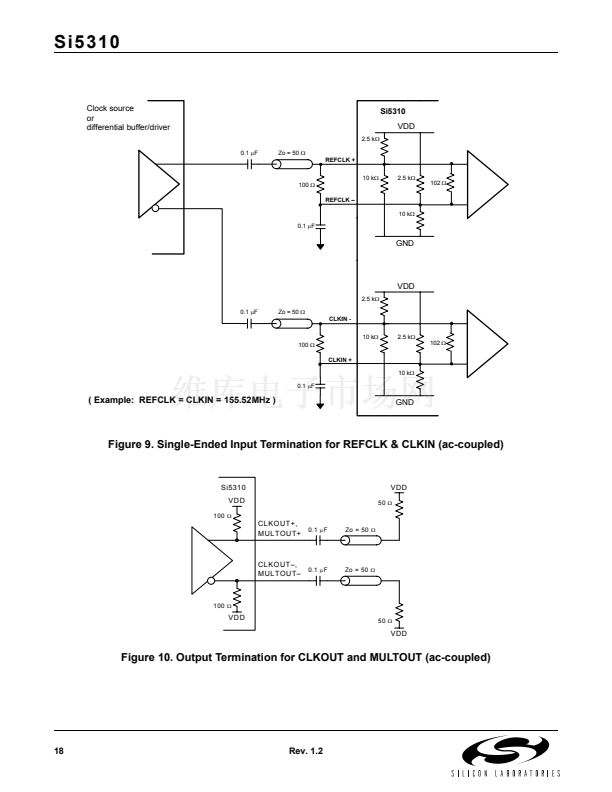
4.13. Differential Output Circuitry
The Si5310 utilizes a current mode logic (CML)
architecture to output both the regenerated clock
(CLKOUT) and the multiplied clock (MULTOUT). An
example of output termination with ac coupling is shown
in Figure 10. For applications in which direct dc coupling
is possible, the 0.1
碌F
capacitors may be omitted. The
differential peak-to-peak voltage swing of the CML is
listed in Table 2 on page 6.
4.12. Differential Input Circuitry
The Si5310 provides differential inputs for both the input
clock (CLKIN) and the reference clock (REFCLK)
inputs. An example termination for these inputs is
shown in Figure 6. In applications where direct dc
16
Rev. 1.2


 1
1
 2
2
 3
3
 4
4
 5
5
 6
6
 7
7
 8
8
 9
9
 10
10
 11
11
 12
12
 13
13
 14
14
 15
15
 16
16
 17
17
 18
18
 19
19
 20
20
 21
21
 22
22
 23
23
 24
24
 25
25
 26
26
