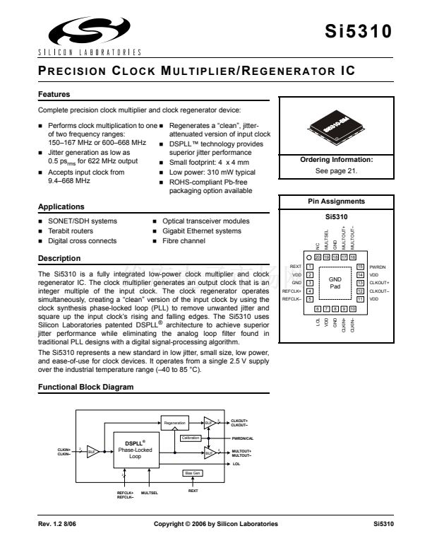
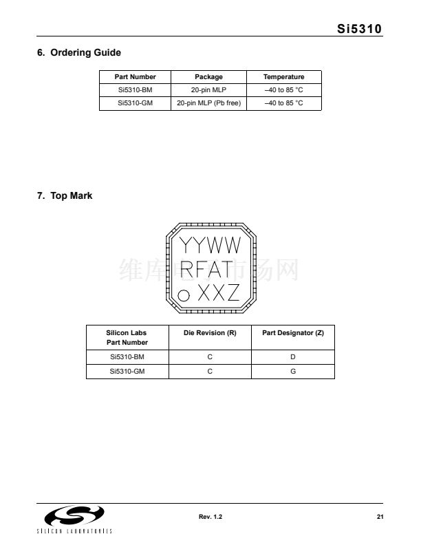
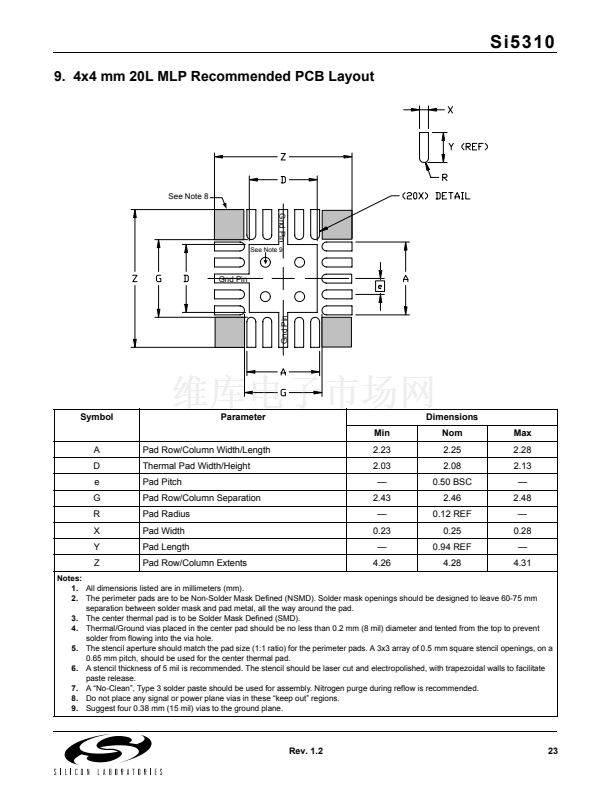
Figure 11. Si5310 Pin Configuration
Table 11. Si5310 Pin Descriptions
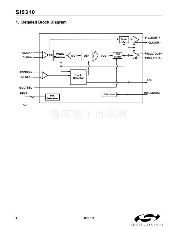
External Bias Resistor.
bias currents within the device. This pin must be
connected to GND through a 10 k鈩?/div>
(1%)
resistor.
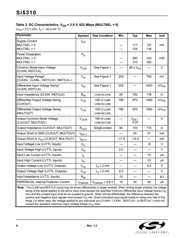
2.5 V
GND
Supply Voltage.
Nominally 2.5 V.
Supply Ground.
Nominally 0.0 V. The GND pad found on the bottom
of the 20-pin micro leaded package (see Figure 12)
must be connected directly to supply ground.
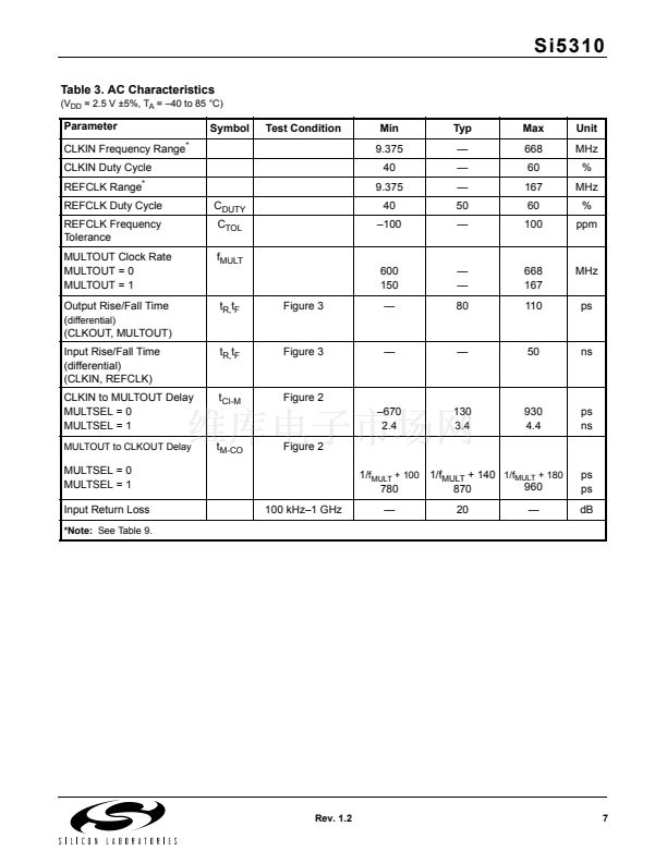
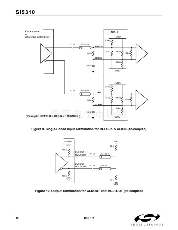
Differential Reference Clock.
The reference clock sets the initial operating fre-
quency used by the onboard PLL for clock regenera-
tion and multiplication. Additionally, the reference
clock is used as a reference in generation of the LOL
output and to bound the frequency drift of MULTOUT
when CLKIN is not present.
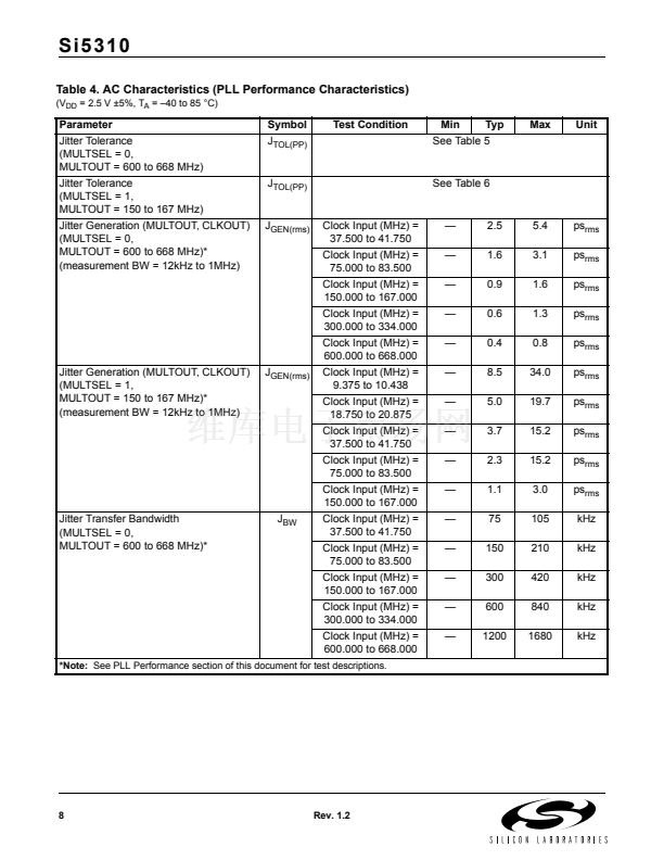
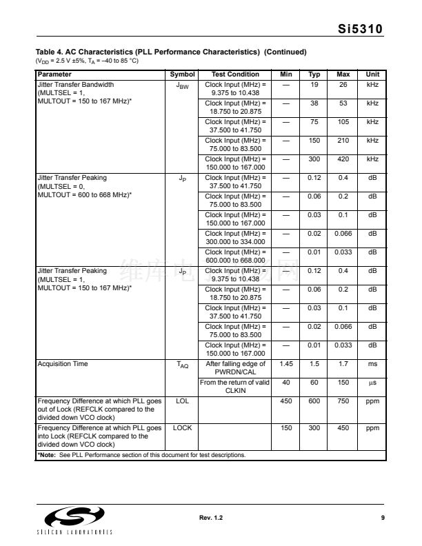
Loss of Lock.
This output is driven high when a divided version of
the clock multiplier output deviates from the refer-
ence clock frequency by the amount specified in
Table 4 on page 8.
Differential Clock Input.
Differential input clock from which MULTOUT is
derived.
2, 7, 11, 14
3, 8, 18, and
GND Pad
VDD
GND
4, 5
REFCLK+, REF-
CLK鈥?/div>
I
See Table 2
6
LOL
O
LVTTL
9, 10
CLKIN+, CLKIN鈥?/div>
I
See Table 2
Rev. 1.2
19


 1
1
 2
2
 3
3
 4
4
 5
5
 6
6
 7
7
 8
8
 9
9
 10
10
 11
11
 12
12
 13
13
 14
14
 15
15
 16
16
 17
17
 18
18
 19
19
 20
20
 21
21
 22
22
 23
23
 24
24
 25
25
 26
26
