Cyclone FPGA Family Data Sheet
Preliminary Information
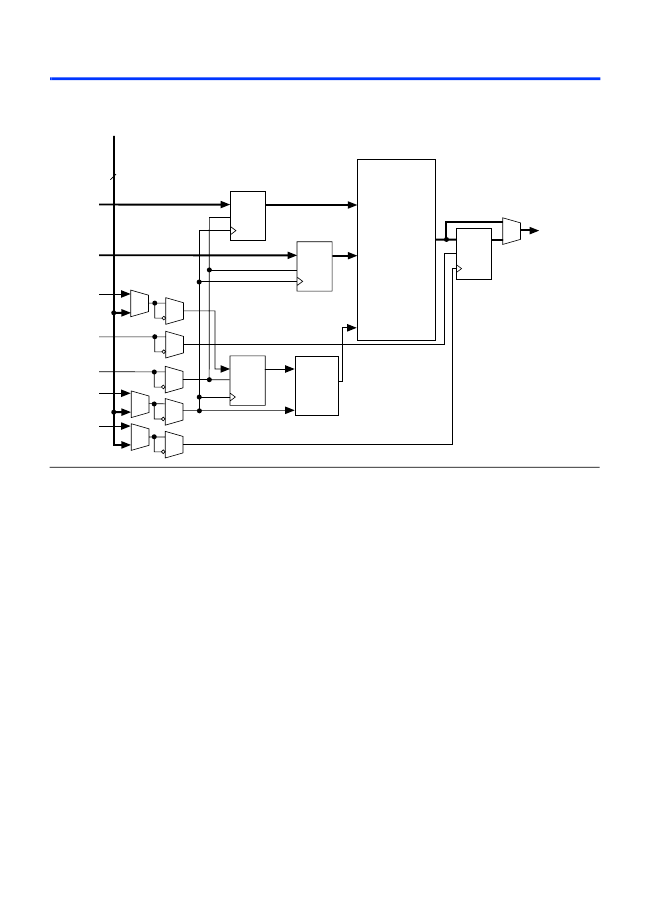
Figure 21. Single-Port Mode
6 LAB Row
Clocks
6
data[ ]
D
Q
ENA
RAM/ROM
256
脳
16
512
脳
8
1,024
脳
4
Data In
2,048
脳
2
4,096
脳
1
Data Out
D
Q
ENA
To MultiTrack
Interconnect
address[ ]
D
Q
ENA
Address
wren
Write Enable
outclken
inclken
inclock
D
Q
ENA
Write
Pulse
Generator
outclock
Global Clock
Network &
Phase-Locked
Loops
Cyclone devices provide a global clock network and up to two PLLs for a
complete clock management solution.
Global Clock Network
There are four dedicated clock pins (CLK[3..0], two pins on the left side
and two pins on the right side) that drive the global clock network, as
shown in
Figure 22.
PLL outputs, logic array, and dual-purpose clock
(DPCLK[7..0]) pins can also drive the global clock network.
The eight global clock lines in the global clock network drive throughout
the entire device. The global clock network can provide clocks for all
resources within the device铮OEs, LEs, and memory blocks. The global
clock lines can also be used for control signals, such as clock enables and
synchronous or asynchronous clears fed from the external pin, or DQS
signals for DDR SDRAM or FCRAM interfaces. Internal logic can also
drive the global clock network for internally generated global clocks and
asynchronous clears, clock enables, or other control signals with large
fanout.
Figure 22
shows the various sources that drive the global clock
network.
34
Altera Corporation


 1
1
 2
2
 3
3
 4
4
 5
5
 6
6
 7
7
 8
8
 9
9
 10
10
 11
11
 12
12
 13
13
 14
14
 15
15
 16
16
 17
17
 18
18
 19
19
 20
20
 21
21
 22
22
 23
23
 24
24
 25
25
 26
26
 27
27
 28
28
 29
29
 30
30
 31
31
 32
32
 33
33
 34
34
 35
35
 36
36
 37
37
 38
38
 39
39
 40
40
 41
41
 42
42
 43
43
 44
44
 45
45
 46
46
 47
47
 48
48
 49
49
 50
50
 51
51
 52
52
 53
53
 54
54
 55
55
 56
56
 57
57
 58
58
 59
59
 60
60
 61
61
 62
62
 63
63
 64
64
 65
65
 66
66
 67
67
 68
68
 69
69
 70
70
 71
71
 72
72
 73
73
 74
74
 75
75
 76
76
 77
77
 78
78
 79
79
 80
80
 81
81
 82
82
 83
83
 84
84
 85
85
 86
86
 87
87
 88
88
 89
89
 90
90
 91
91
 92
92
 93
93
 94
94
