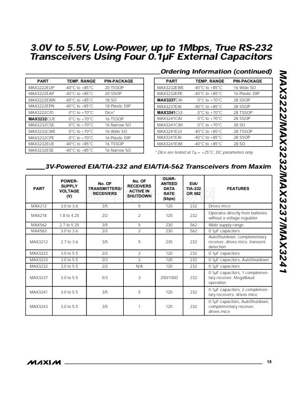
3.0V to 5.5V, Low-Power, up to 1Mbps, True RS-232
Transceivers Using Four 0.1碌F External Capacitors
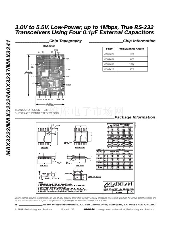
MAX3222/MAX3232/MAX3237/MAX3241
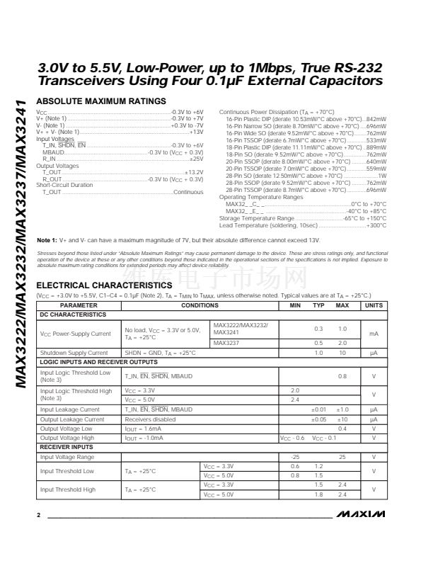
ABSOLUTE MAXIMUM RATINGS
V
CC
...........................................................................-0.3V to +6V
V+ (Note 1) ...............................................................-0.3V to +7V
V- (Note 1) ................................................................+0.3V to -7V
V+ + V- (Note 1)...................................................................+13V
Input Voltages
T_IN,
SHDN, EN
...................................................-0.3V to +6V
MBAUD...................................................-0.3V to (V
CC
+ 0.3V)
R_IN .................................................................................卤25V
Output Voltages
T_OUT...........................................................................卤13.2V
R_OUT ....................................................-0.3V to (V
CC
+ 0.3V)
Short-Circuit Duration
T_OUT ....................................................................Continuous
Continuous Power Dissipation (T
A
= +70掳C)
16-Pin Plastic DIP (derate 10.53mW/掳C above +70掳C)...842mW
16-Pin Narrow SO (derate 8.70mW/掳C above +70掳C) ....696mW
16-Pin Wide SO (derate 9.52mW/掳C above +70掳C)........762mW
16-Pin TSSOP (derate 6.7mW/掳C above +70掳C).............533mW
18-Pin Plastic DIP (derate 11.11mW/掳C above +70掳C) ..889mW
18-Pin SO (derate 9.52mW/掳C above +70掳C)..............762mW
20-Pin SSOP (derate 8.00mW/掳C above +70掳C) .........640mW
20-Pin TSSOP (derate 7.0mW/掳C above +70掳C).............559mW
28-Pin SO (derate 12.50mW/掳C above +70掳C) .....................1W
28-Pin SSOP (derate 9.52mW/掳C above +70掳C) .........762mW
28-Pin TSSOP (derate 8.7mW/掳C above +70掳C).............696mW
Operating Temperature Ranges
MAX32_ _C_ _.....................................................0掳C to +70掳C
MAX32_ _E_ _ .................................................-40掳C to +85掳C
Storage Temperature Range .............................-65掳C to +150掳C
Lead Temperature (soldering, 10sec) .............................+300掳C
Note 1:
V+ and V- can have a maximum magnitude of 7V, but their absolute difference cannot exceed 13V.
Stresses beyond those listed under 鈥淎bsolute Maximum Ratings鈥?may cause permanent damage to the device. These are stress ratings only, and functional
operation of the device at these or any other conditions beyond those indicated in the operational sections of the specifications is not implied. Exposure to
absolute maximum rating conditions for extended periods may affect device reliability.
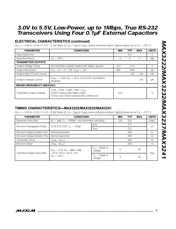
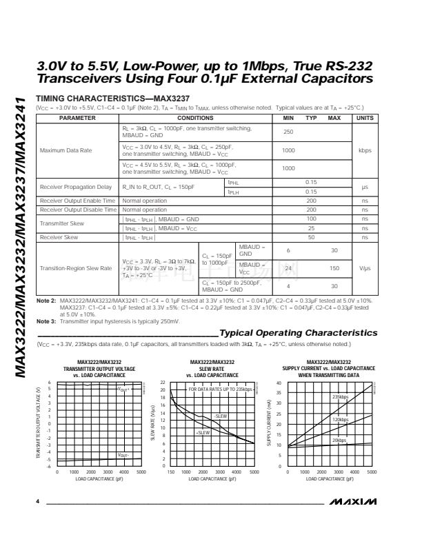
ELECTRICAL CHARACTERISTICS
(V
CC
= +3.0V to +5.5V, C1鈥揅4 = 0.1碌F (Note 2), T
A
= T
MIN
to T
MAX
, unless otherwise noted. Typical values are at T
A
= +25掳C.)
PARAMETER
DC CHARACTERISTICS
V
CC
Power-Supply Current
Shutdown Supply Current
Input Logic Threshold Low
(Note 3)
Input Logic Threshold High
(Note 3)
Input Leakage Current
Output Leakage Current
Output Voltage Low
Output Voltage High
RECEIVER INPUTS
Input Voltage Range
Input Threshold Low
Input Threshold High
T
A
= +25掳C
T
A
= +25掳C
V
CC
= 5.0V
V
CC
= 3.3V
V
CC
= 5.0V
V
CC
= 3.3V
V
CC
= 5.0V
-25
0.6
0.8
1.2
1.5
1.5
1.8
2.4
2.4
25
V
V
V
No load, V
CC
= 3.3V or 5.0V,
T
A
= +25掳C
SHDN = GND, T
A
= +25掳C
MAX3222/MAX3232/
MAX3241
MAX3237
0.3
0.5
1.0
1.0
2.0
10
碌A
mA
CONDITIONS
MIN
TYP
MAX
UNITS
LOGIC INPUTS AND RECEIVER OUTPUTS
T_IN,
EN, SHDN,
MBAUD
V
CC
= 3.3V
V
CC
= 5.0V
T_IN,
EN, SHDN,
MBAUD
Receivers disabled
I
OUT
= 1.6mA
I
OUT
= -1.0mA
V
CC
- 0.6
V
CC
- 0.1
2.0
2.4
卤0.01
卤0.05
卤1.0
卤10
0.4
0.8
V
V
碌A
碌A
V
V
2
_______________________________________________________________________________________


 1
1
 2
2
 3
3
 4
4
 5
5
 6
6
 7
7
 8
8
 9
9
 10
10
 11
11
 12
12
 13
13
 14
14
 15
15
 16
16
