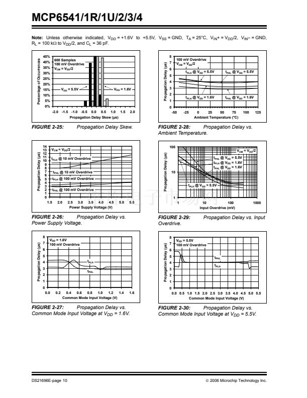
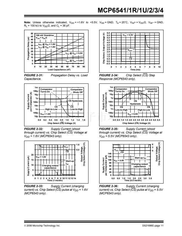
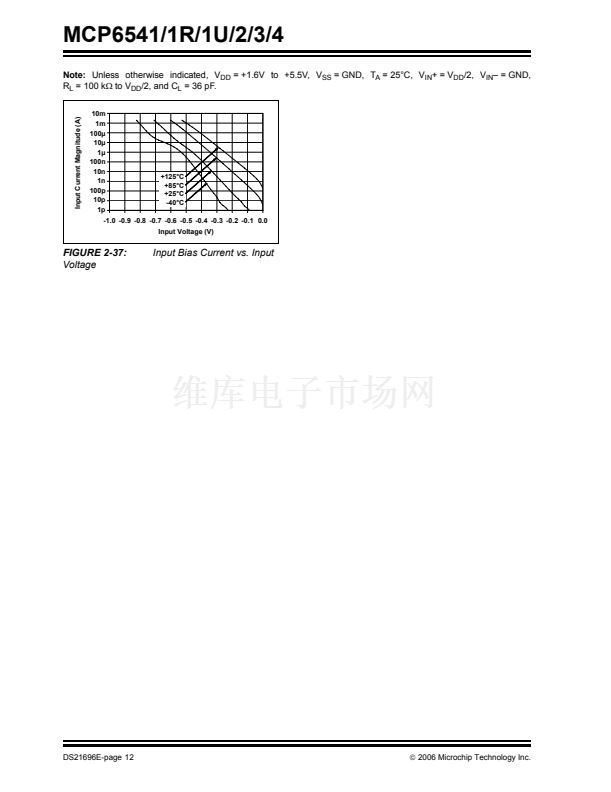
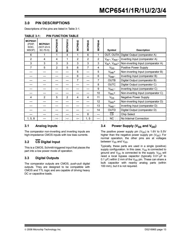
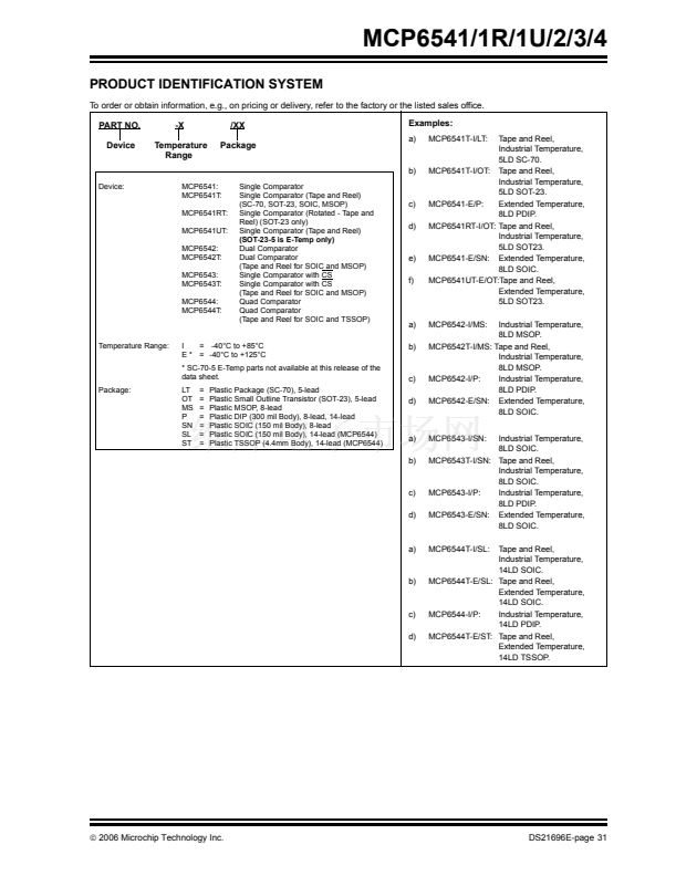
鈥?/div>
OUTD
CS
NC
Positive Power Supply
Non-inverting Input (comparator B)
Inverting Input (comparator B)
Digital Output (comparator B)
Digital Output (comparator C)
Inverting Input (comparator C)
Non-inverting Input (comparator C)
Negative Power Supply
Non-inverting Input (comparator D)
Inverting Input (comparator D)
Digital Output (comparator D)
Chip Select
No Internal Connection
3.1
Analog Inputs
3.4
Power Supply (V
SS
and V
DD
)
The comparator non-inverting and inverting inputs are
high-impedance CMOS inputs with low bias currents.
3.2
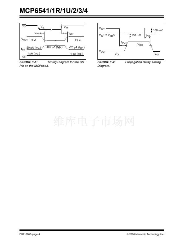
CS Digital Input
The positive power supply pin (V
DD
) is 1.6V to 5.5V
higher than the negative power supply pin (V
SS
). For
normal operation, the other pins are at voltages
between V
SS
and V
DD
.
Typically, these parts are used in a single (positive)
supply configuration. In this case, V
SS
is connected to
ground and V
DD
is connected to the supply. V
DD
will
need a local bypass capacitor (typically 0.01 碌F to
0.1 碌F) within 2 mm of the V
DD
pin. These can share a
bulk capacitor with nearby analog parts (within
100 mm), but it is not required.
This is a CMOS, Schmitt-triggered input that places the
part into a low power mode of operation.
3.3
Digital Outputs
The comparator outputs are CMOS, push-pull digital
outputs. They are designed to be compatible with
CMOS and TTL logic and are capable of driving heavy
DC or capacitive loads.
漏
2006 Microchip Technology Inc.
DS21696E-page 13


 1
1
 2
2
 3
3
 4
4
 5
5
 6
6
 7
7
 8
8
 9
9
 10
10
 11
11
 12
12
 13
13
 14
14
 15
15
 16
16
 17
17
 18
18
 19
19
 20
20
 21
21
 22
22
 23
23
 24
24
 25
25
 26
26
 27
27
 28
28
 29
29
 30
30
 31
31
 32
32
 33
33
 34
34
