CMOS transistors at the input. They are designed to
the supply voltages.
inversion.
鈥?/div>
V
OUT
4.1.2
INPUT VOLTAGE AND CURRENT
LIMITS
The ESD protection on the inputs can be depicted as
shown in
Figure 4-1.
This structure was chosen to pro-
tect the input transistors, and to minimize input bias
current (IB). The input ESD diodes clamp the inputs
when they try to go more than one diode drop below
V
SS
. They also clamp any voltages that go too far
above V
DD
; their breakdown voltage is high enough to
allow normal operation, and low enough to bypass ESD
events within the specified limits.
Bond
Pad
V
SS
鈥?(minimum expected V
1
)
2 mA
V
SS
鈥?(minimum expected V
2
)
2 mA
FIGURE 4-2:
Protecting the Analog Inputs.
V
DD
It is also possible to connect the diodes to the left of the
resistors R
1
and R
2
. In this case, the currents through
the diodes D
1
and D
2
need to be limited by some other
mechanism. The resistor then serves as in-rush current
limiter; the DC current into the input pins (V
IN
+ and
V
IN
鈥? should be very small.
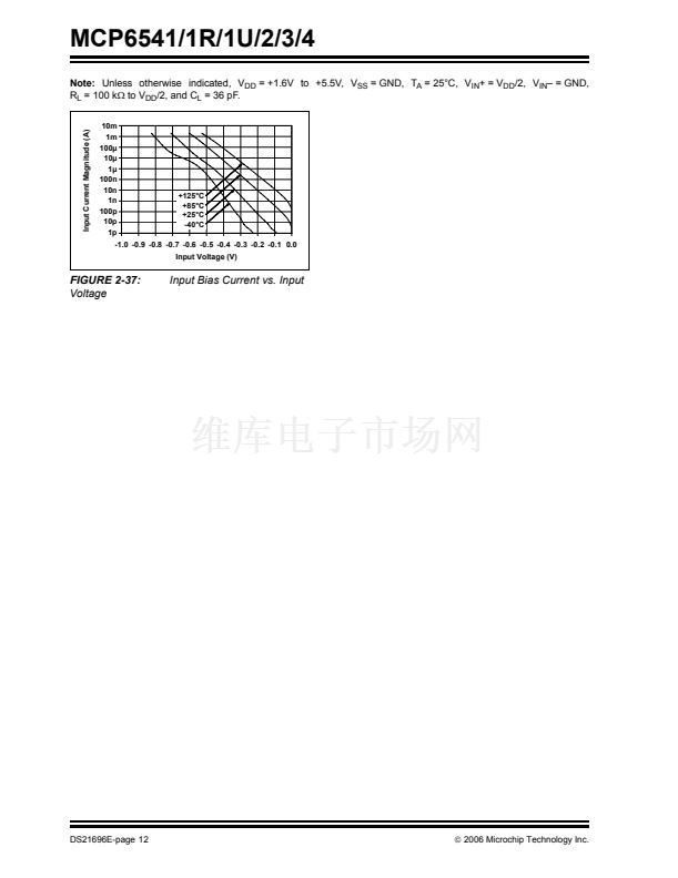
A significant amount of current can flow out of the
inputs when the common mode voltage (V
CM
) is below
ground (V
SS
); see
Figure 2-37.
Applications that are
high impedance may need to limit the useable voltage
range.
V
IN
+ Bond
Pad
Input
Stage
Bond
Pad
V
IN
鈥?/div>
4.1.3
V
SS
Bond
Pad
NORMAL OPERATION
FIGURE 4-1:
Structures.
Simplified Analog Input ESD
In order to prevent damage and/or improper operation
of these amplifiers, the circuits they are in must limit the
currents (and voltages) at the V
IN
+ and V
IN
鈥?pins (see
Absolute Maximum Ratings 鈥?/span>
at the beginning of
Section 1.0 鈥淓lectrical Characteristics鈥?.
Figure 4-3
shows the recommended approach to protecting these
inputs. The internal ESD diodes prevent the input pins
(V
IN
+ and V
IN
鈥? from going too far below ground, and
The input stage of this family of devices uses two
differential input stages in parallel: one operates at low
input voltages and the other at high input voltages. With
this topology, the input voltage is 0.3V above V
DD
and
0.3V below V
SS
. Therefore, the input offset voltage is
measured at both V
SS
- 0.3V and V
DD
+ 0.3V to ensure
proper operation.
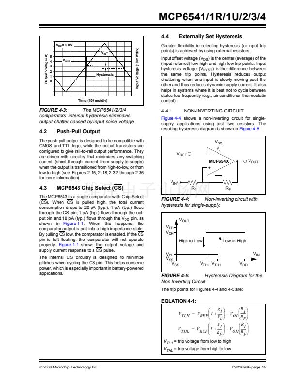
The MCP6541/1R/1U/2/3/4 family has internally-set
hysteresis that is small enough to maintain input offset
accuracy (<7 mV) and large enough to eliminate output
chattering caused by the comparator鈥檚 own input noise
voltage (200 碌V
p-p
).
Figure 4-3
depicts this behavior.
DS21696E-page 14
漏
2006 Microchip Technology Inc.


 1
1
 2
2
 3
3
 4
4
 5
5
 6
6
 7
7
 8
8
 9
9
 10
10
 11
11
 12
12
 13
13
 14
14
 15
15
 16
16
 17
17
 18
18
 19
19
 20
20
 21
21
 22
22
 23
23
 24
24
 25
25
 26
26
 27
27
 28
28
 29
29
 30
30
 31
31
 32
32
 33
33
 34
34
