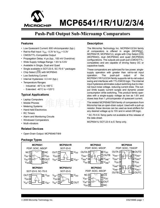
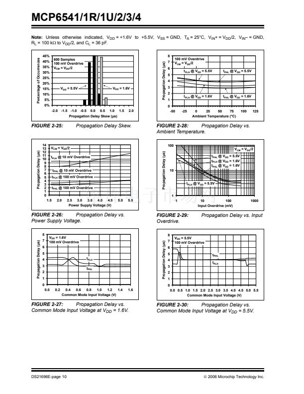
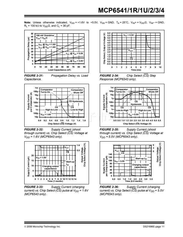
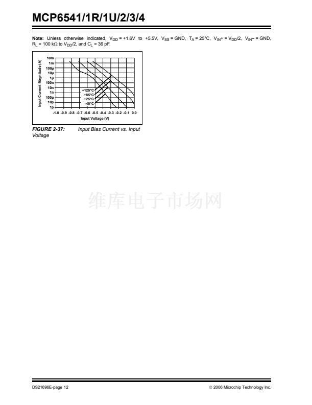
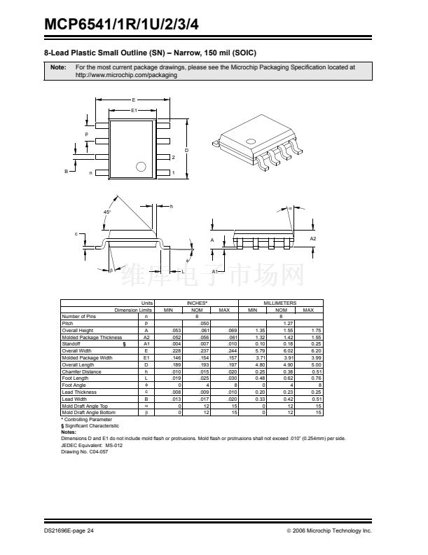
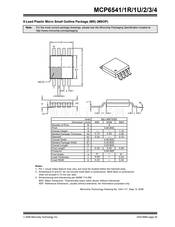
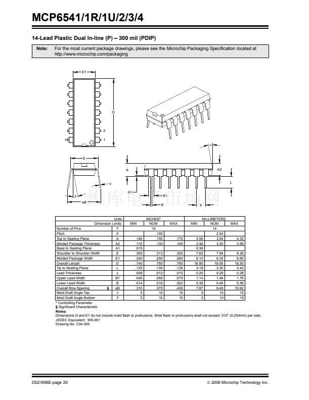
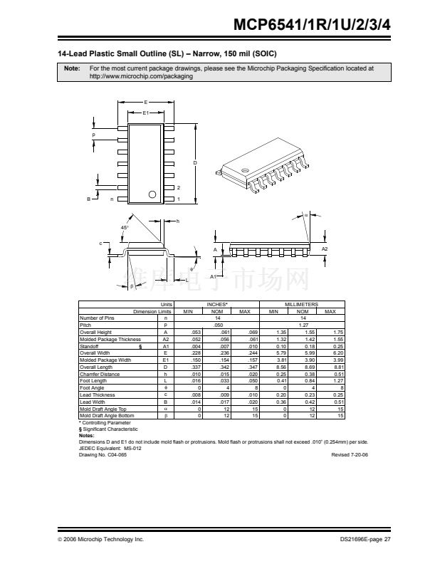
鈳?/div>
R
3
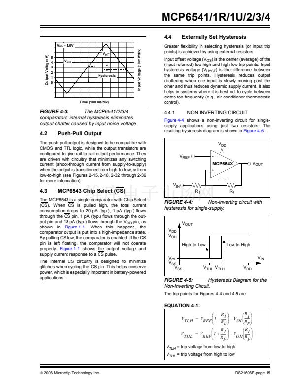
FIGURE 4-6:
Hysteresis.
V
OUT
V
DD
V
OH
Low-to-High
V
OL
V
SS
V
SS
Inverting Circuit With
V
TLH
= trip voltage from low to high
V
THL
= trip voltage from high to low
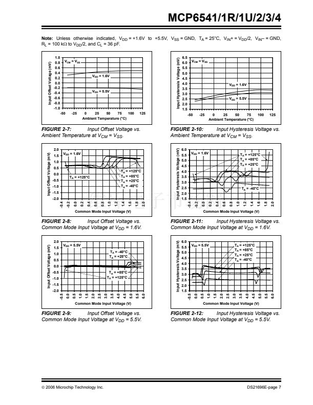
Figure 2-20
and
Figure 2-23
can be used to determine
typical values for V
OH
and V
OL
.
High-to-Low
V
IN
4.5
Bypass Capacitors
V
TLH
V
THL
V
DD
FIGURE 4-7:
Inverting Circuit.
Hysteresis Diagram for the
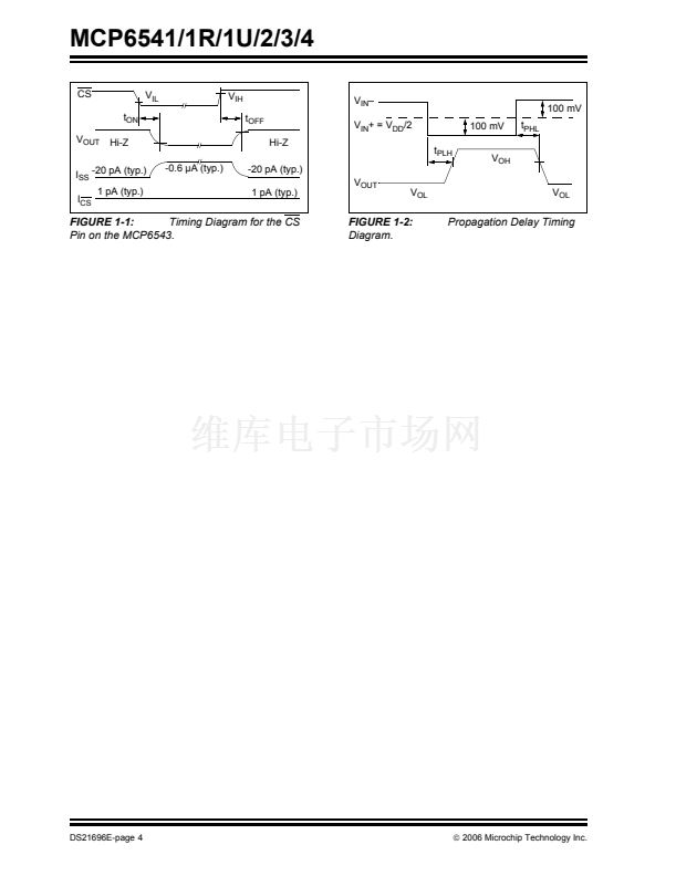
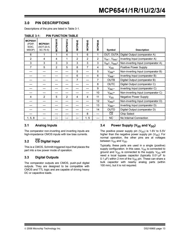
With this family of comparators, the power supply pin
(V
DD
for single supply) should have a local bypass
capacitor (i.e., 0.01 碌F to 0.1 碌F) within 2 mm for good
edge rate performance.
4.6
Capacitive Loads
In order to determine the trip voltages (V
THL
and V
TLH
)
for the circuit shown in
Figure 4-6,
R
2
and R
3
can be
simplified to the Thevenin equivalent circuit with
respect to V
DD
, as shown in
Figure 4-8.
V
DD
-
MCP654X
+
V
SS
V
23
R
23
R
F
V
OUT
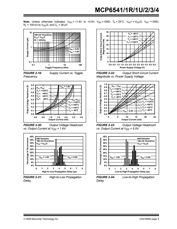
Reasonable capacitive loads (e.g., logic gates) have
little impact on propagation delay (see
Figure 2-31).
The supply current increases with increasing toggle
frequency (Figure
2-19),
especially with higher
capacitive loads.
4.7
Battery Life
In order to maximize battery life in portable
applications, use large resistors and small capacitive
loads. Avoid toggling the output more than necessary.
Do not use Chip Select (CS) frequently to conserve
start-up power. Capacitive loads will draw additional
power at start-up.
FIGURE 4-8:
Thevenin Equivalent Circuit.
DS21696E-page 16
漏
2006 Microchip Technology Inc.


 1
1
 2
2
 3
3
 4
4
 5
5
 6
6
 7
7
 8
8
 9
9
 10
10
 11
11
 12
12
 13
13
 14
14
 15
15
 16
16
 17
17
 18
18
 19
19
 20
20
 21
21
 22
22
 23
23
 24
24
 25
25
 26
26
 27
27
 28
28
 29
29
 30
30
 31
31
 32
32
 33
33
 34
34
