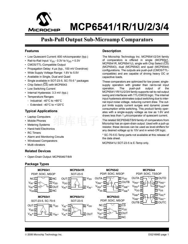
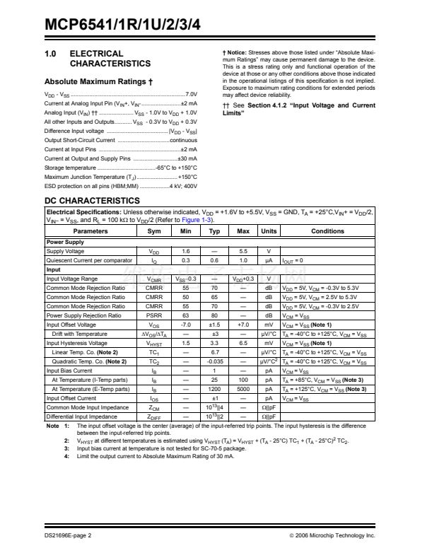
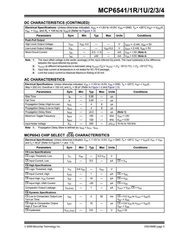
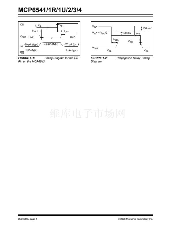
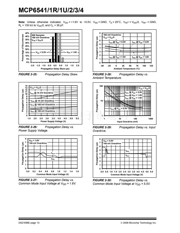
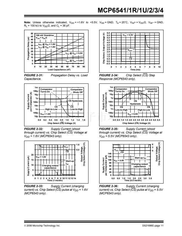
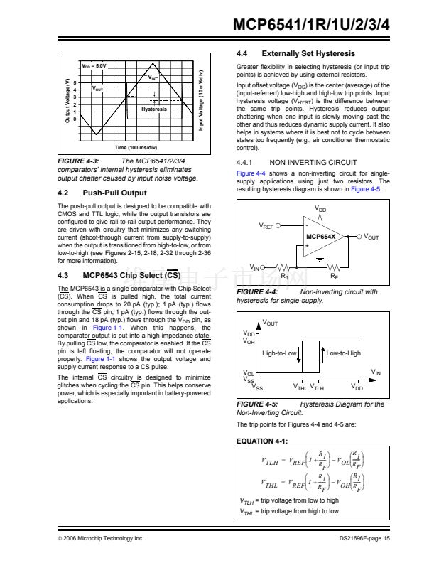
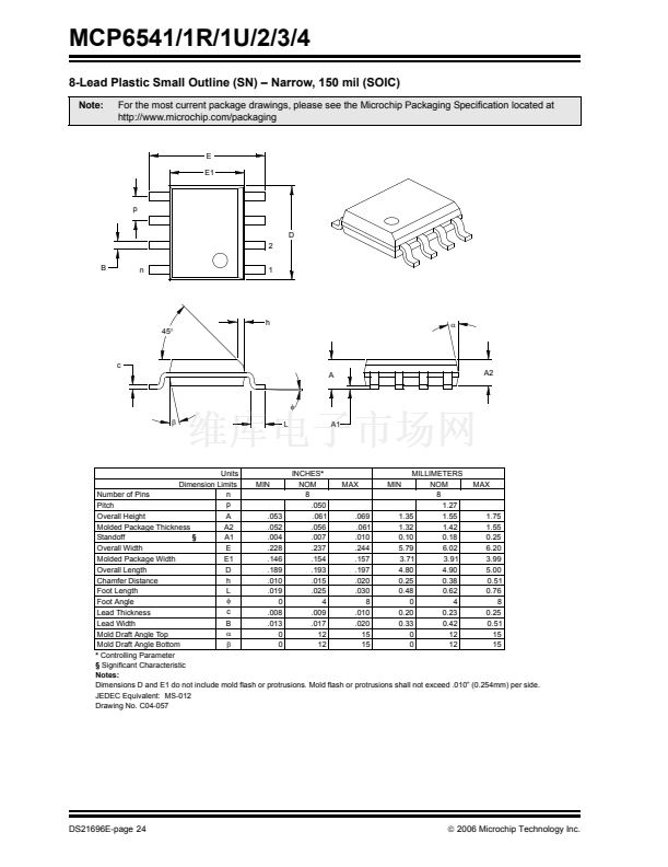
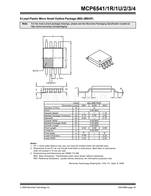
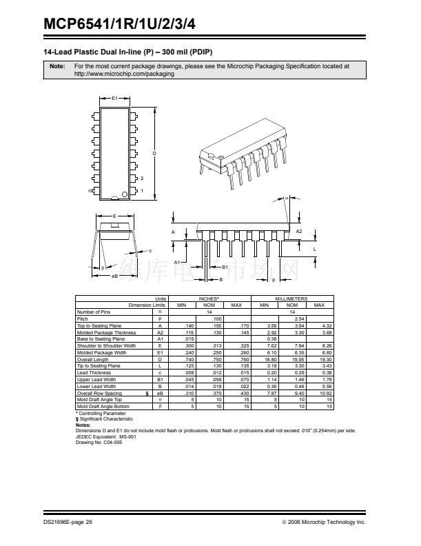
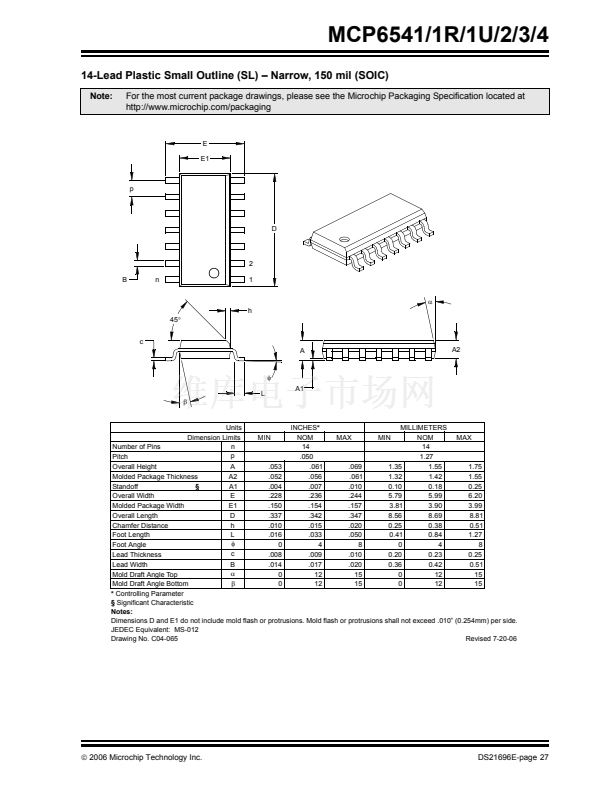
MCP6541/1R/1U/2/3/4
4.8
PCB Surface Leakage
4.9
Unused Comparators
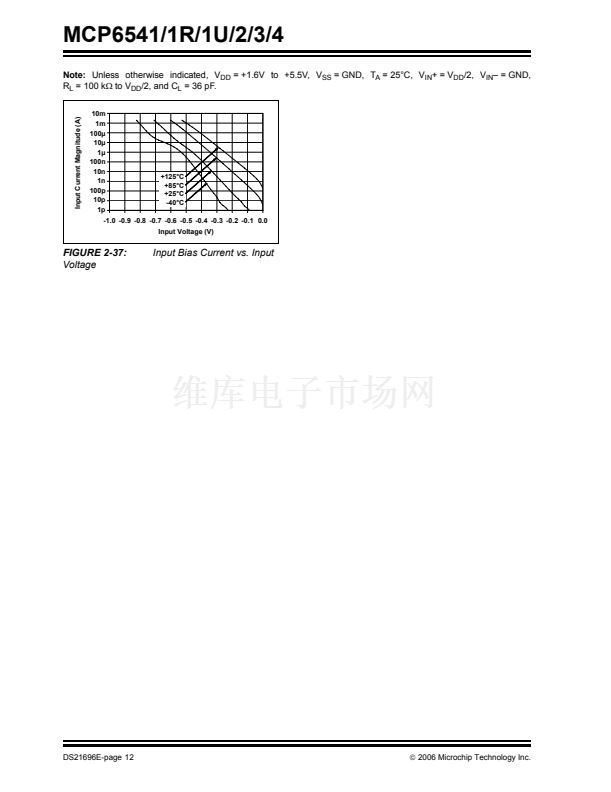
In applications where low input bias current is critical,
PCB (Printed Circuit Board) surface leakage effects
need to be considered. Surface leakage is caused by
humidity, dust or other contamination on the board.
Under low humidity conditions, a typical resistance
between nearby traces is 10
12
惟.
A 5V difference would
cause 5 pA of current to flow. This is greater than the
MCP6541/1R/1U/2/3/4 family鈥檚 bias current at 25掳C
(1 pA, typ.).
The easiest way to reduce surface leakage is to use a
guard ring around sensitive pins (or traces). The guard
ring is biased at the same voltage as the sensitive pin.
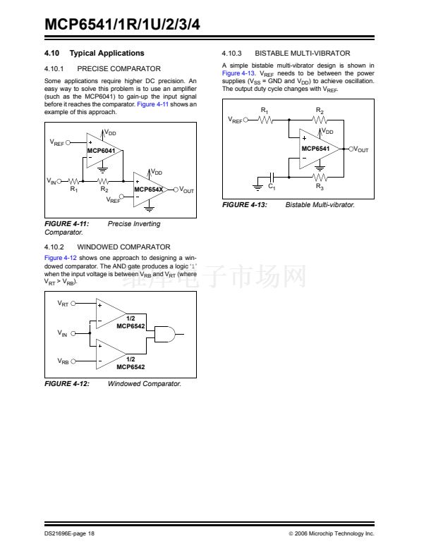
An example of this type of layout is shown in
Figure 4-9.
V
IN
-
V
IN
+
V
SS
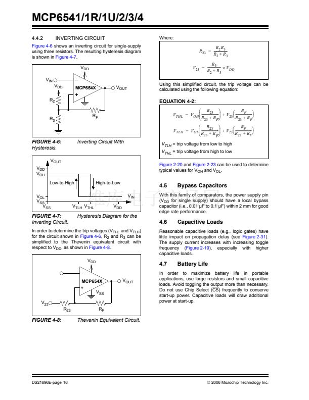
An unused amplifier in a quad package (MCP6544)
should be configured as shown in
Figure 4-10.
This
circuit prevents the output from toggling and causing
crosstalk. It uses the minimum number of components
and draws minimal current (see
Figure 2-15
and
Figure 2-18).
录 MCP6544
V
DD
鈥?/div>
+
FIGURE 4-10:
Guard Ring
Unused Comparators.
FIGURE 4-9:
Example Guard Ring Layout
for Inverting Circuit.
1.
Inverting Configuration (Figures 4-6 and 4-9):
a. Connect the guard ring to the non-inverting
input pin (V
IN
+). This biases the guard ring
to the same reference voltage as the
comparator (e.g., V
DD
/2 or ground).
b. Connect the inverting pin (V
IN
鈥? to the input
pad without touching the guard ring.
Non-inverting Configuration (Figure
4-4):
a. Connect the non-inverting pin (V
IN
+) to the
input pad without touching the guard ring.
b. Connect the guard ring to the inverting input
pin (V
IN
鈥?.
2.
漏
2006 Microchip Technology Inc.
DS21696E-page 17


 1
1
 2
2
 3
3
 4
4
 5
5
 6
6
 7
7
 8
8
 9
9
 10
10
 11
11
 12
12
 13
13
 14
14
 15
15
 16
16
 17
17
 18
18
 19
19
 20
20
 21
21
 22
22
 23
23
 24
24
 25
25
 26
26
 27
27
 28
28
 29
29
 30
30
 31
31
 32
32
 33
33
 34
34
