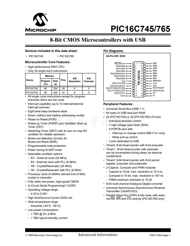
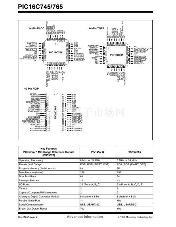
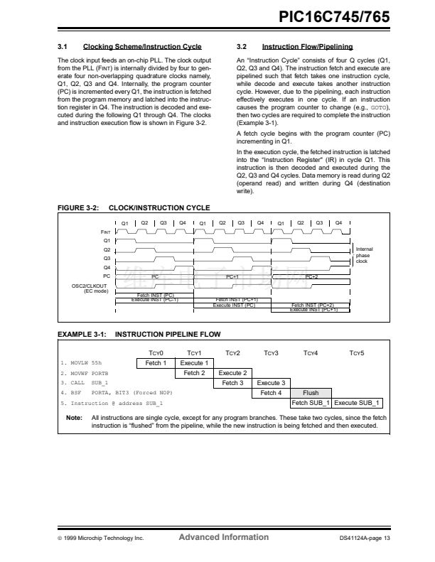
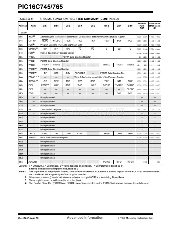
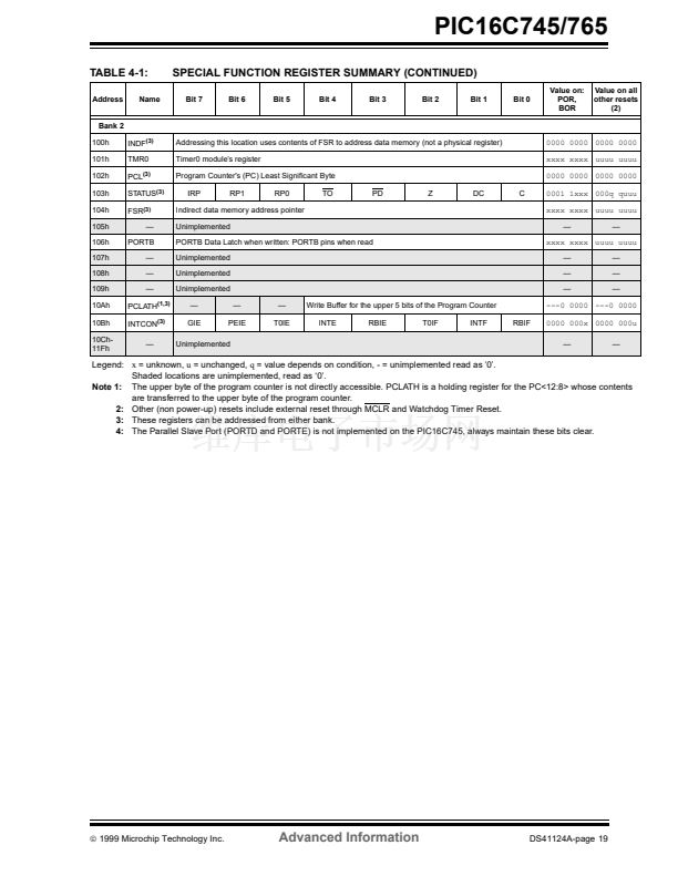
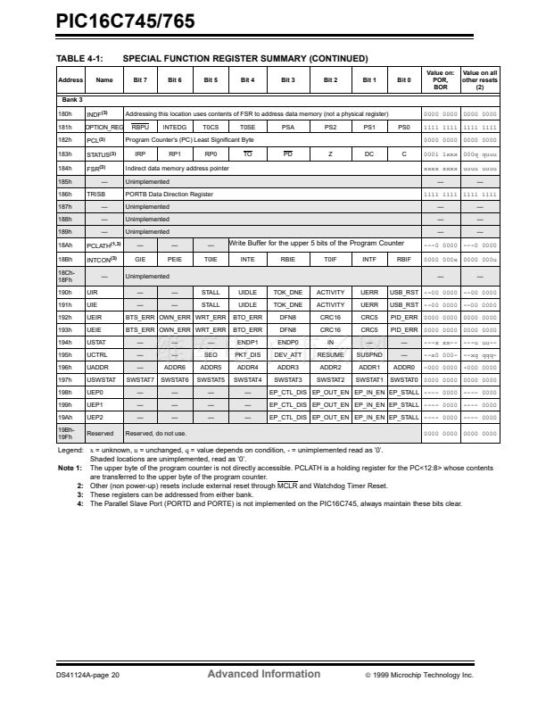
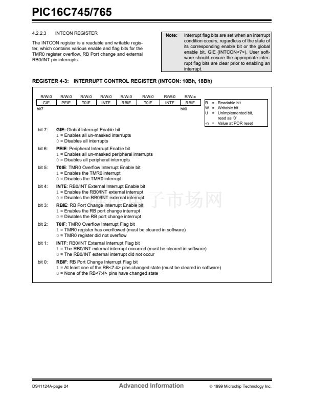
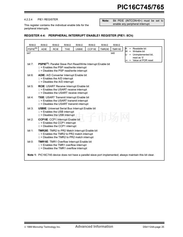
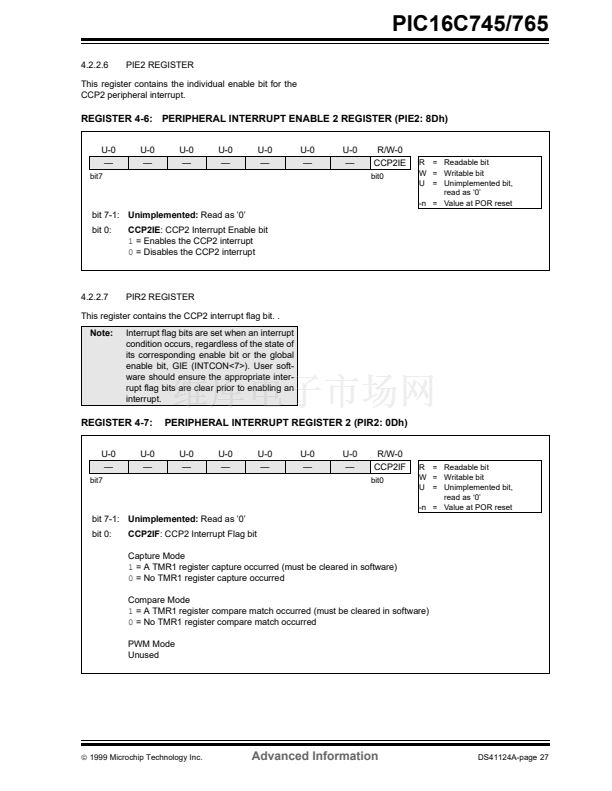
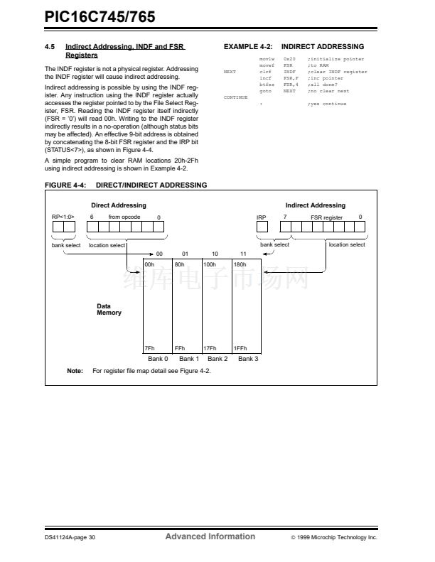
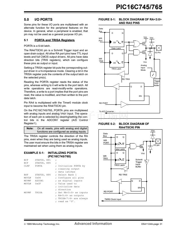
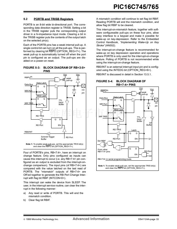
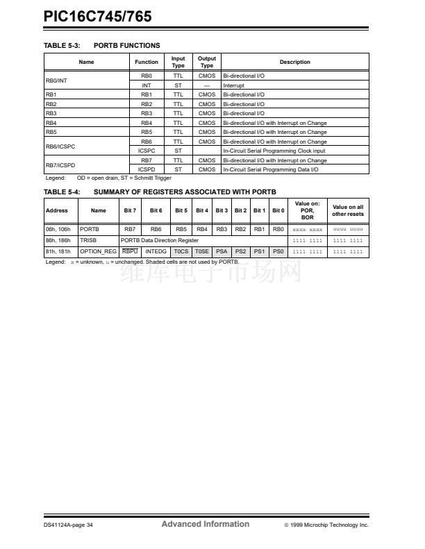
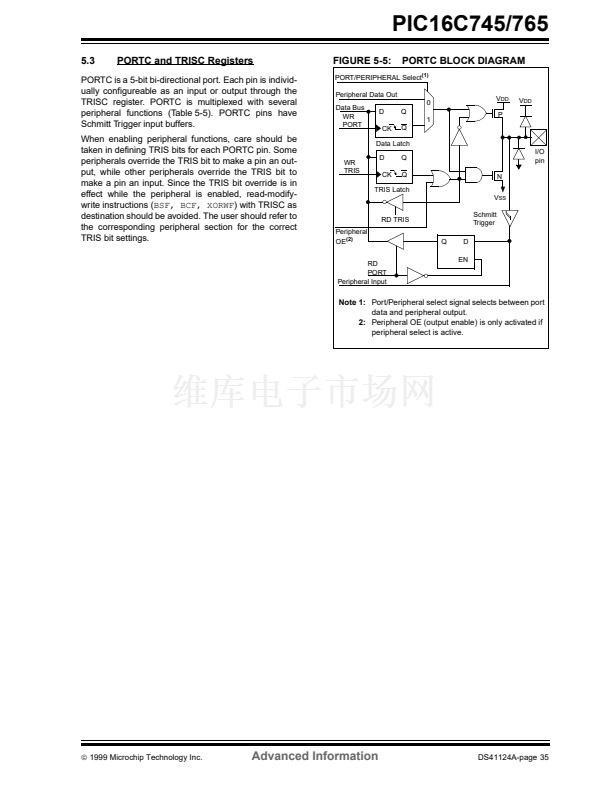
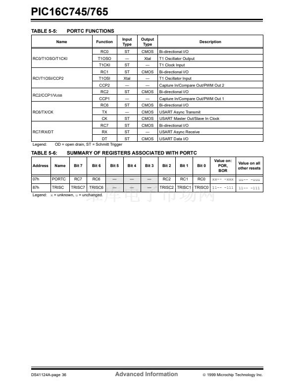
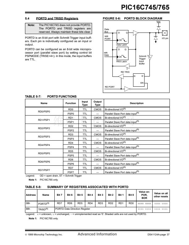
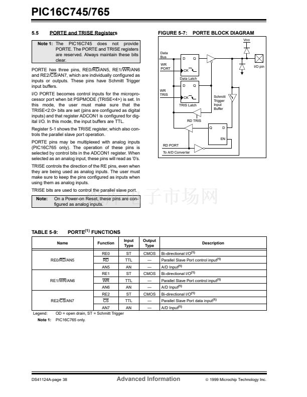
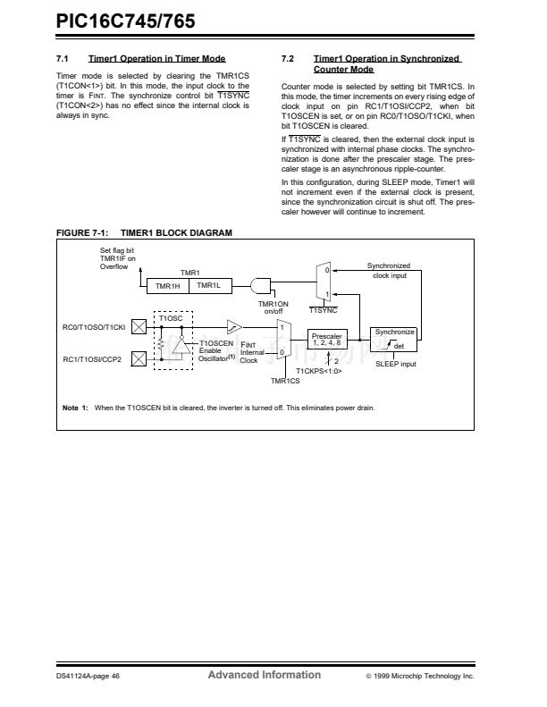
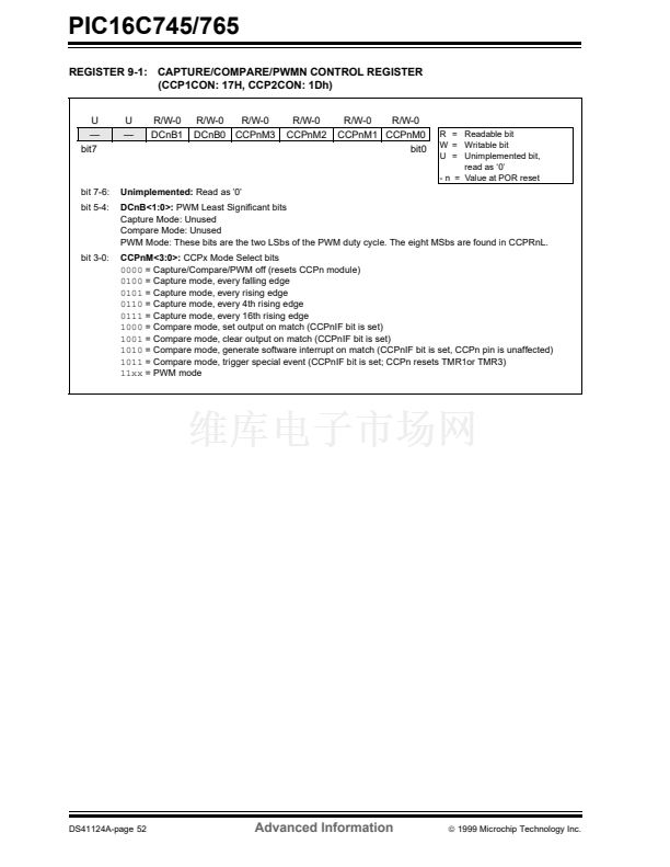
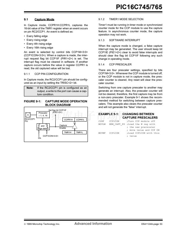
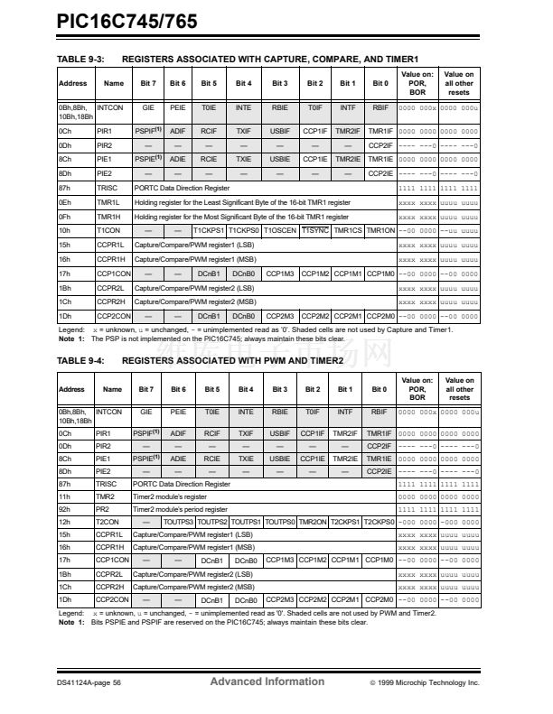
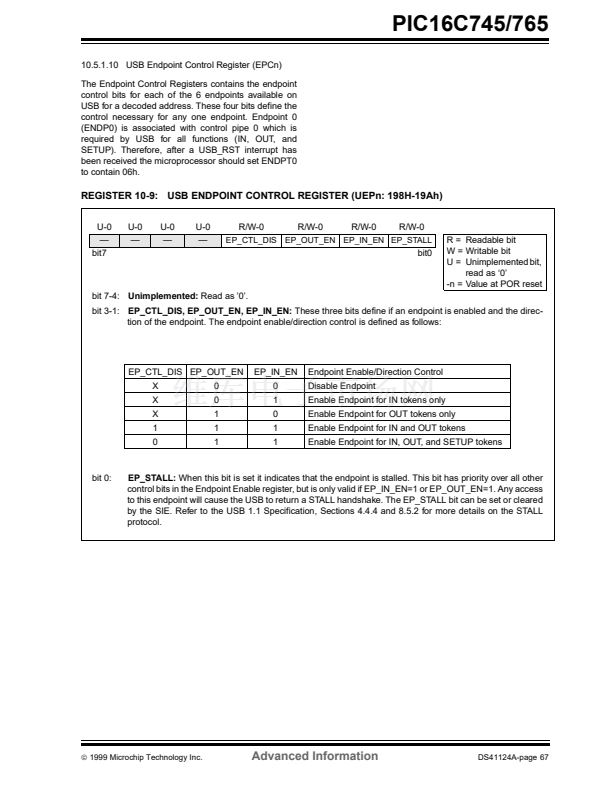
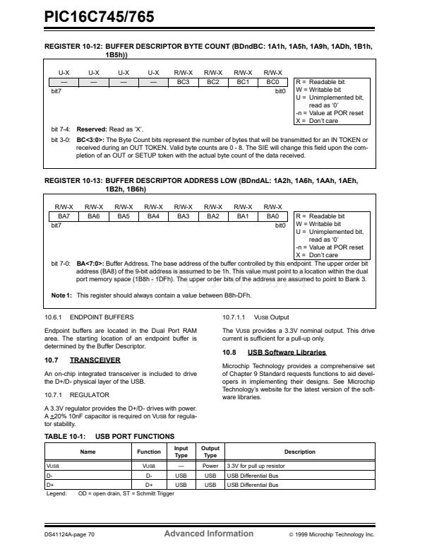
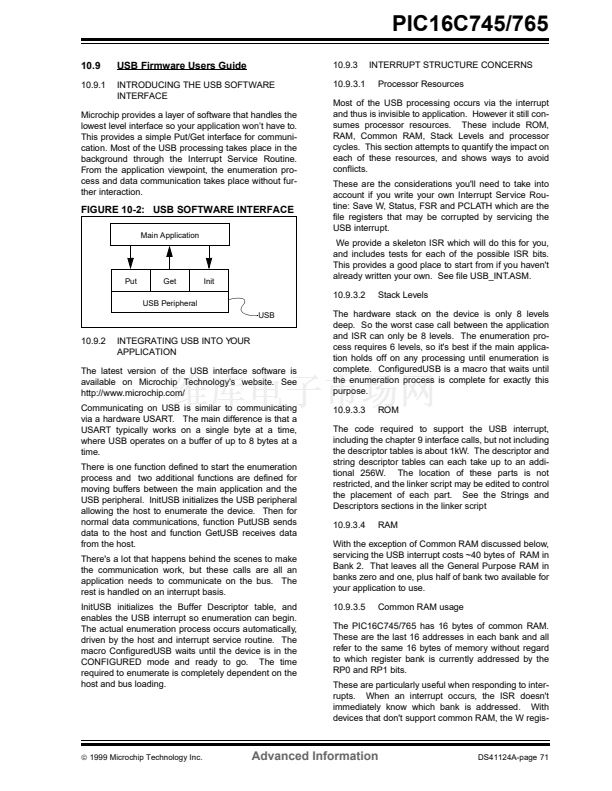
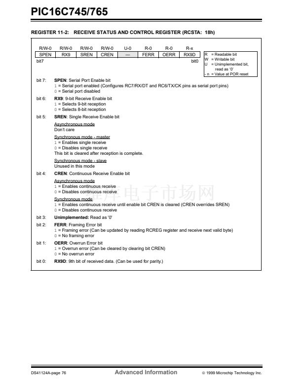
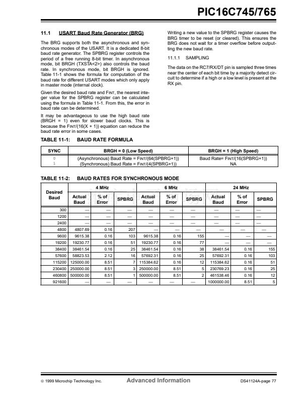
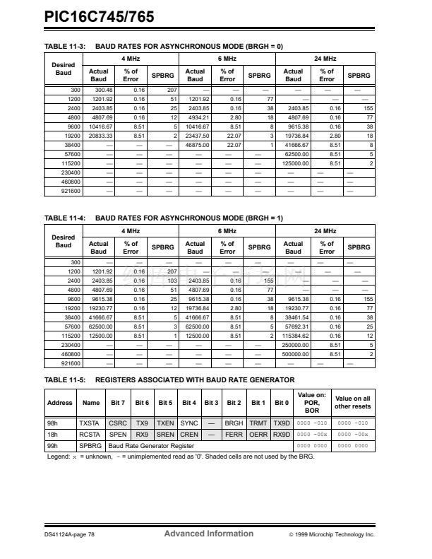
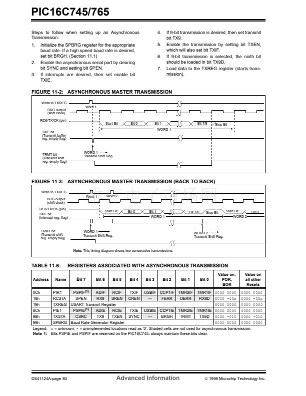
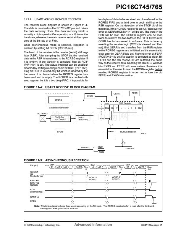
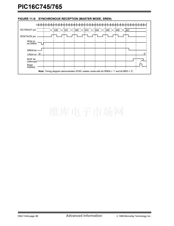
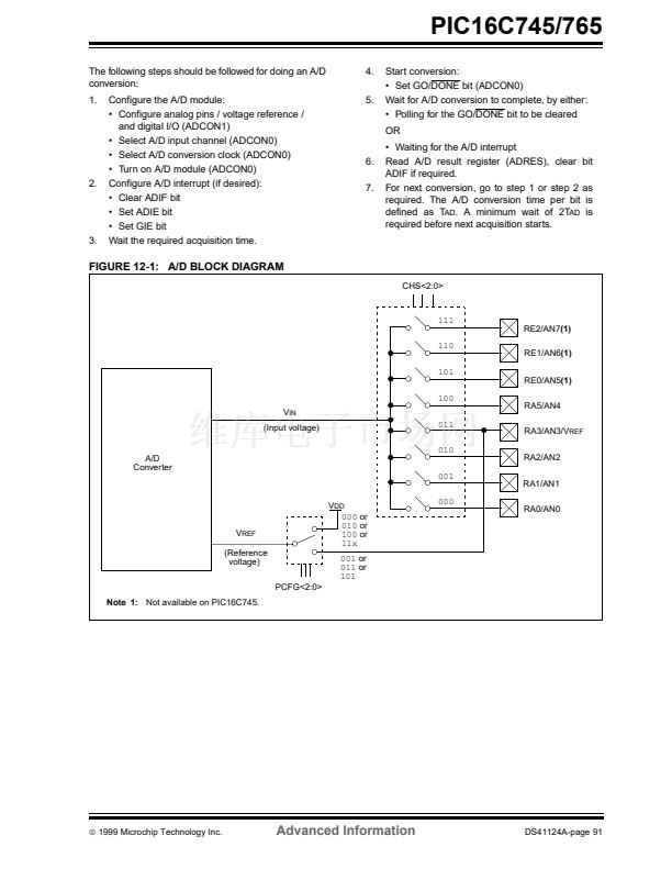
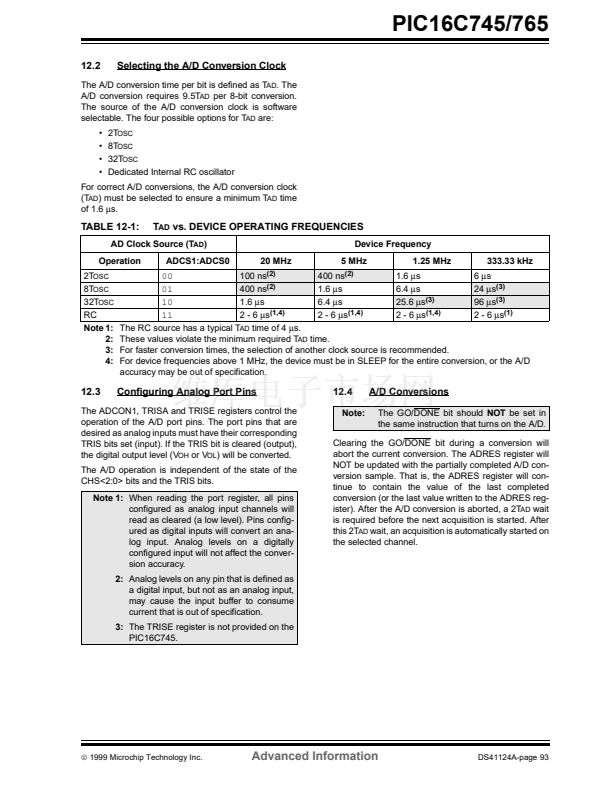
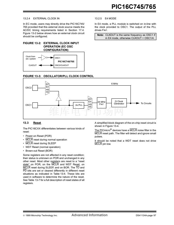
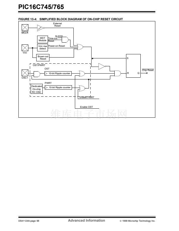
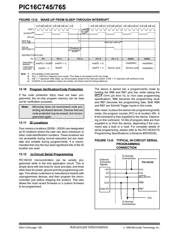
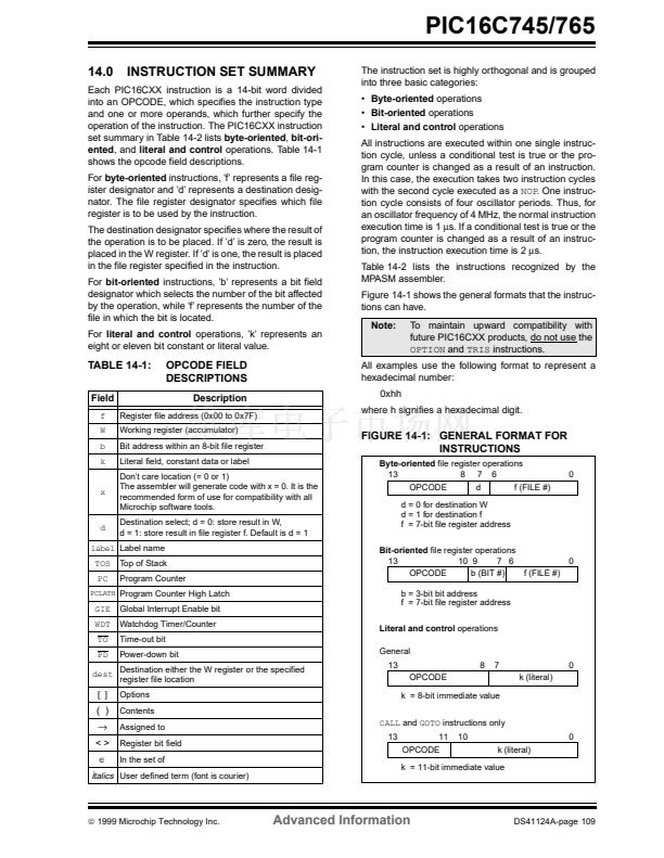
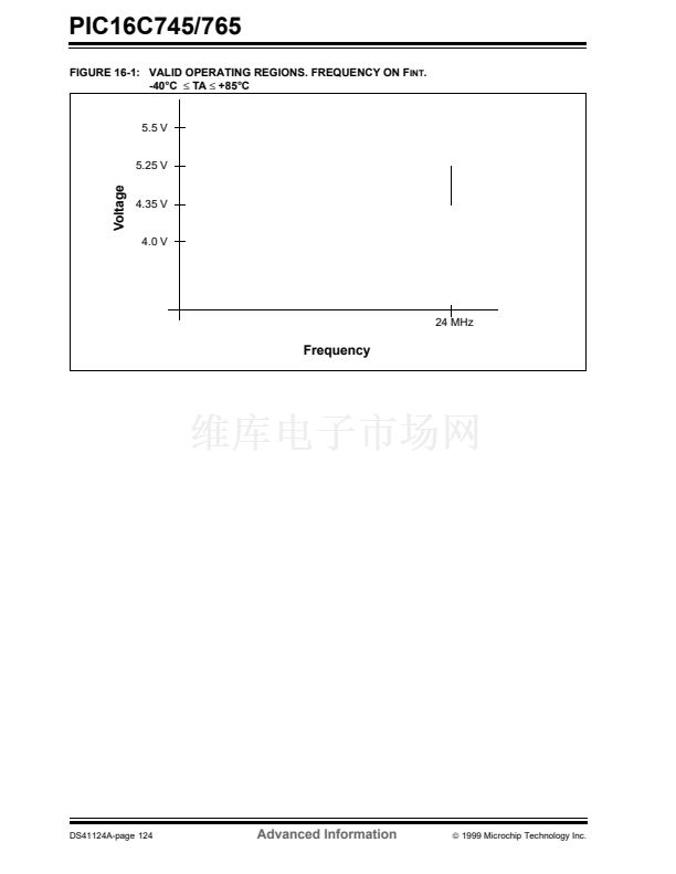
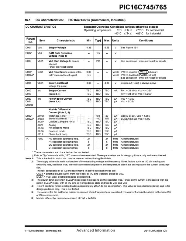
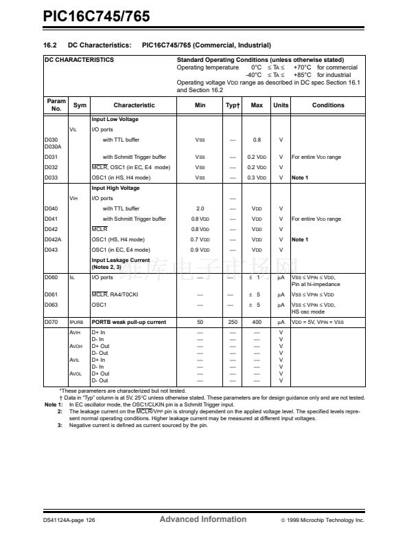
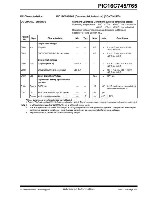
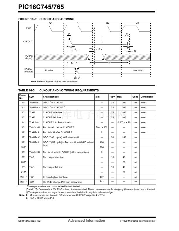
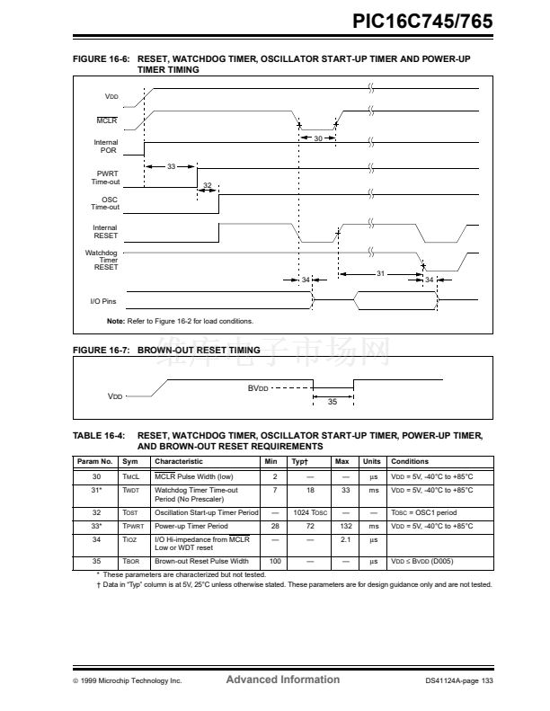
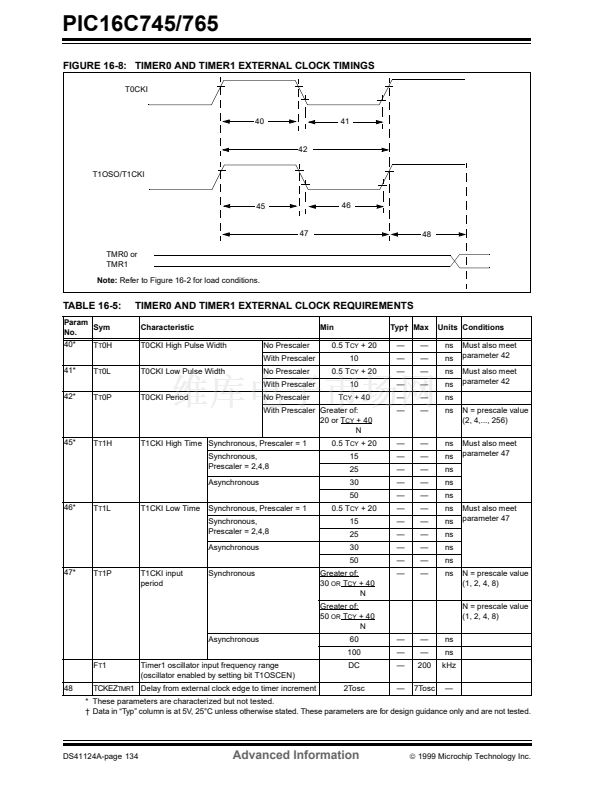
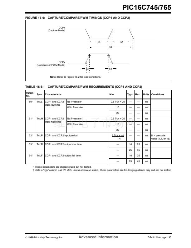
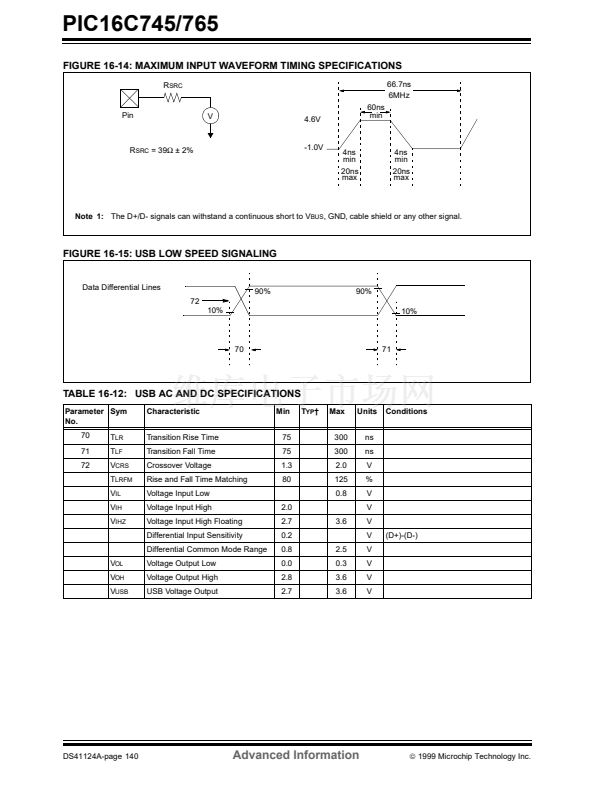
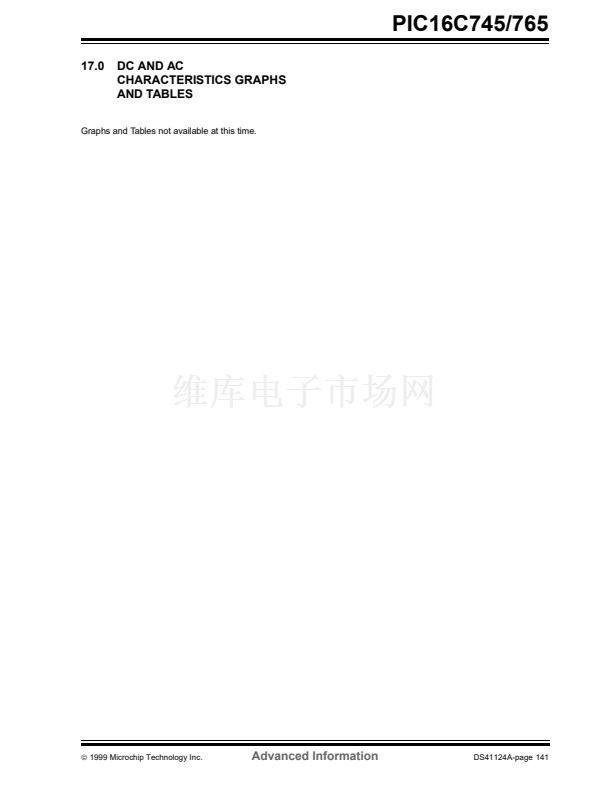
PIC16C745/765
6.2
Using Timer0 with an External Clock
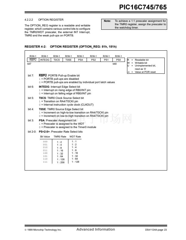
The PSA and PS<2:0> bits (OPTION_REG<3:0>) deter-
mine the prescaler assignment and prescale ratio.
When assigned to the Timer0 module, all instructions
writing to the TMR0 register (e.g.
CLRF 1, MOVWF 1,
BSF 1,x....etc.)
will clear the prescaler. When assigned
to WDT, a
CLRWDT
instruction will clear the prescaler
along with the watchdog timer. The prescaler is not
readable or writable.
Note:
Writing to TMR0, when the prescaler is
assigned to Timer0, will clear the prescaler
count, but will not change the prescaler
assignment.
When no prescaler is used, the external clock input is
the same as the prescaler output. The synchronization
of T0CKI with the internal phase clocks is accom-
plished by sampling the prescaler output on the Q2 and
Q4 cycles of the internal phase clocks. Therefore, it is
necessary for T0CKI to be high for at least 2Tosc (and
a small RC delay of 20 ns) and low for at least 2Tosc
(and a small RC delay of 20 ns). Refer to the electrical
specification of the desired device.
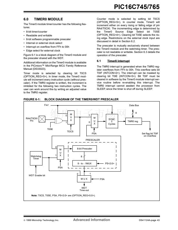
6.3
Prescaler
There is only one prescaler available which is mutually
exclusively shared between the Timer0 module and the
watchdog timer. A prescaler assignment for the Timer0
module means that there is no prescaler for the watch-
dog timer, and vice-versa. This prescaler is not readable
or writable (see Figure 6-1).
To avoid an unintended device RESET, the following
instruction sequence (shown in Example 6-1) must be
executed when changing the prescaler assignment
from Timer0 to the WDT. This sequence must be fol-
lowed even if the WDT is disabled.
EXAMPLE 6-1:
CHANGING PRESCALER (TIMER0鈫扺DT)
1)
BSF
MOVLW
MOVWF
BCF
CLRF
BSF
MOVLW
MOVWF
CLRWDT
b鈥檟xxx1xxx鈥?/div>
OPTION_REG
STATUS, RP0
STATUS, RP0
b鈥檟x0x0xxx鈥?/div>
OPTION_REG
STATUS, RP0
TMR0
STATUS, RP1
b鈥檟xxx1xxx鈥?/div>
OPTION_REG
;Bank1
;Select clock source and prescale value of
;other than 1:1
;Bank0
;Clear TMR0 and prescaler
;Bank1
;Select WDT, do not change prescale value
;
;Clears WDT and prescaler
;Select new prescale value and WDT
;
;Bank0
2)
3)
4)
5)
6)
7)
8)
9)
Lines 2 and 3 do
NOT have to be
included if the final
desired prescale
value is other than
1:1. If 1:1 is the final
desired value, then a
temporary prescale
value is set in lines 2
and 3 and the final
prescale value will
be set in lines 10
and 11.
10) MOVLW
11) MOVWF
12) BCF
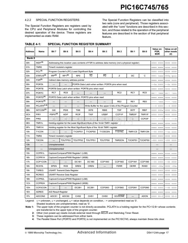
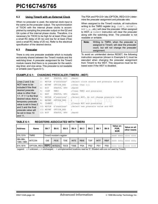
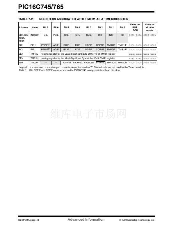
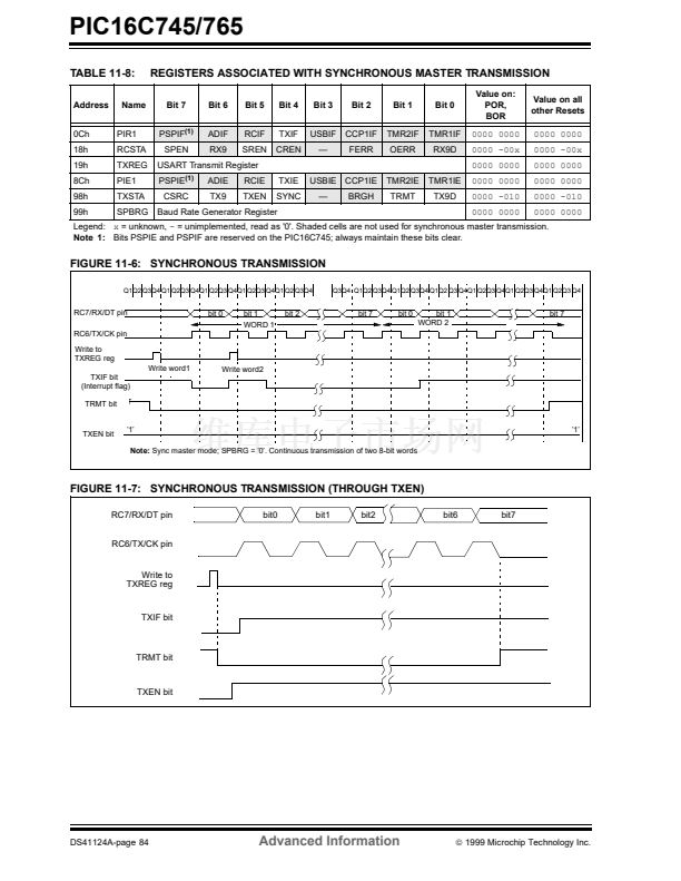
TABLE 6-1:
Address
01h,101h
0Bh,8Bh,
10Bh,18Bh
81h,181h
REGISTERS ASSOCIATED WITH TIMER0
Name
Bit 7
Bit 6
Bit 5
Bit 4
Bit 3
Bit 2
Bit 1
Bit 0
Value on:
POR,
BOR
xxxx xxxx
INTE
T0SE
RBIE
PSA
T0IF
PS2
INTF
PS1
RBIF
PS0
0000 000x
1111 1111
Value on all
other resets
uuuu uuuu
0000 000u
1111 1111
TMR0
INTCON
Timer0 module鈥檚 register
GIE
PEIE
T0IE
T0CS
OPTION_REG RBPU INTEDG
Legend:
x
= unknown,
u
= unchanged,
-
= unimplemented locations read as '0'. Shaded cells are not used by Timer0.
DS41124A-page 44
Advanced Information
漏
1999 Microchip Technology Inc.


 1
1
 2
2
 3
3
 4
4
 5
5
 6
6
 7
7
 8
8
 9
9
 10
10
 11
11
 12
12
 13
13
 14
14
 15
15
 16
16
 17
17
 18
18
 19
19
 20
20
 21
21
 22
22
 23
23
 24
24
 25
25
 26
26
 27
27
 28
28
 29
29
 30
30
 31
31
 32
32
 33
33
 34
34
 35
35
 36
36
 37
37
 38
38
 39
39
 40
40
 41
41
 42
42
 43
43
 44
44
 45
45
 46
46
 47
47
 48
48
 49
49
 50
50
 51
51
 52
52
 53
53
 54
54
 55
55
 56
56
 57
57
 58
58
 59
59
 60
60
 61
61
 62
62
 63
63
 64
64
 65
65
 66
66
 67
67
 68
68
 69
69
 70
70
 71
71
 72
72
 73
73
 74
74
 75
75
 76
76
 77
77
 78
78
 79
79
 80
80
 81
81
 82
82
 83
83
 84
84
 85
85
 86
86
 87
87
 88
88
 89
89
 90
90
 91
91
 92
92
 93
93
 94
94
 95
95
 96
96
 97
97
 98
98
 99
99
 100
100
 101
101
 102
102
 103
103
 104
104
 105
105
 106
106
 107
107
 108
108
 109
109
 110
110
 111
111
 112
112
 113
113
 114
114
 115
115
 116
116
 117
117
 118
118
 119
119
 120
120
 121
121
 122
122
 123
123
 124
124
 125
125
 126
126
 127
127
 128
128
 129
129
 130
130
 131
131
 132
132
 133
133
 134
134
 135
135
 136
136
 137
137
 138
138
 139
139
 140
140
 141
141
 142
142
 143
143
 144
144
 145
145
 146
146
 147
147
 148
148
 149
149
 150
150
 151
151
 152
152
 153
153
 154
154
 155
155
 156
156
 157
157
 158
158
