鈥?/div>
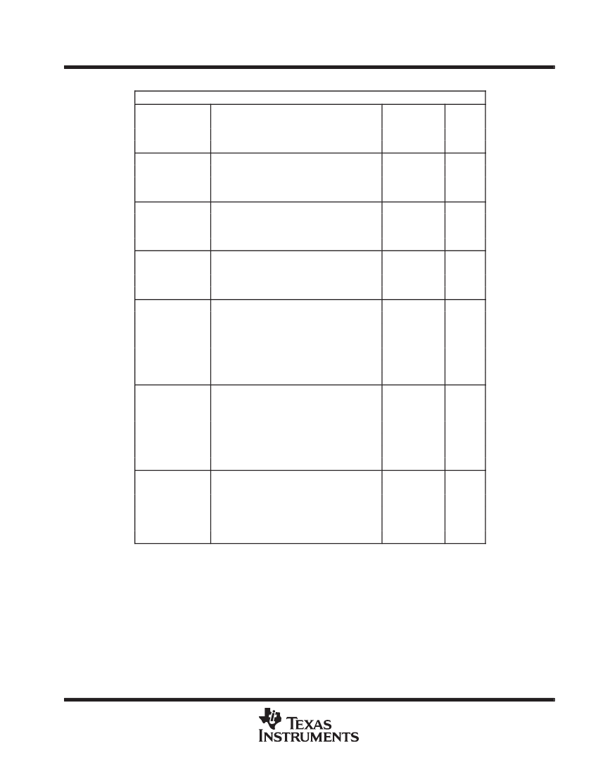
Voltage applied at V
CC
to V
SS
. . . . . . . . . . . . . . . . . . . . . . . . . . . . . . . . . . . . . . . . . . . . . . . . . . . . 鈭?.3 V to + 4.1 V
Voltage applied to any pin (see Note) . . . . . . . . . . . . . . . . . . . . . . . . . . . . . . . . . . . . . . . . . . 鈭?.3 V to V
CC
+ 0.3 V
Diode current at any device terminal . . . . . . . . . . . . . . . . . . . . . . . . . . . . . . . . . . . . . . . . . . . . . . . . . . . . . . .
卤2
mA
Storage temperature (unprogrammed device) . . . . . . . . . . . . . . . . . . . . . . . . . . . . . . . . . . . . . . . 鈭?5掳C to 150掳C
Storage temperature (programmed device) . . . . . . . . . . . . . . . . . . . . . . . . . . . . . . . . . . . . . . . . . . 鈭?0掳C to 85掳C
鈥?Stresses beyond those listed under 鈥渁bsolute maximum ratings鈥?may cause permanent damage to the device. These are stress ratings only, and
functional operation of the device at these or any other conditions beyond those indicated under 鈥渞ecommended operating conditions鈥?is not
implied. Exposure to absolute-maximum-rated conditions for extended periods may affect device reliability.
NOTE:
All voltages referenced to VSS. The JTAG fuse-blow voltage, VFB, is allowed to exceed the absolute maximum rating. The voltage is
applied to the TDI/TCLK pin when blowing the JTAG fuse.
POST OFFICE BOX 655303
鈥?/div>
DALLAS, TEXAS 75265
17


 1
1
 2
2
 3
3
 4
4
 5
5
 6
6
 7
7
 8
8
 9
9
 10
10
 11
11
 12
12
 13
13
 14
14
 15
15
 16
16
 17
17
 18
18
 19
19
 20
20
 21
21
 22
22
 23
23
 24
24
 25
25
 26
26
 27
27
 28
28
 29
29
 30
30
 31
31
 32
32
 33
33
 34
34
 35
35
 36
36
 37
37
 38
38
 39
39
 40
40
 41
41
 42
42
 43
43
 44
44
 45
45
 46
46
 47
47
 48
48
 49
49
 50
50
 51
51
 52
52
 53
53
