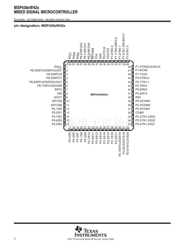
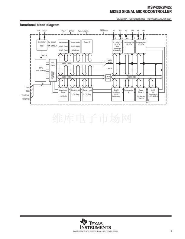
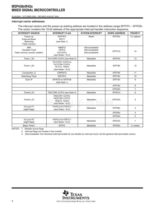
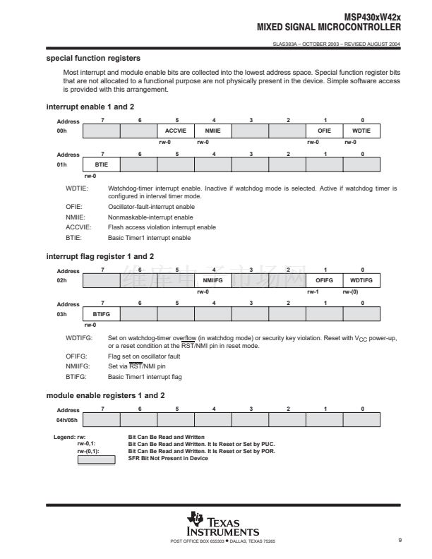
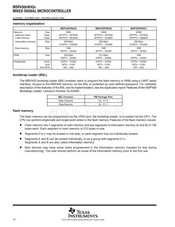
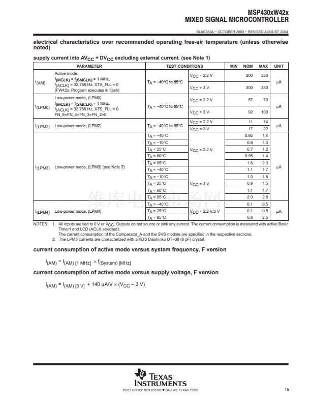
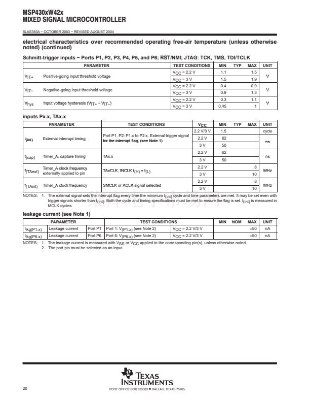
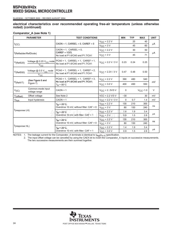
MSP430xW42x
MIXED SIGNAL MICROCONTROLLER
SLAS383A 鈭?OCTOBER 2003 鈭?REVISED AUGUST 2004
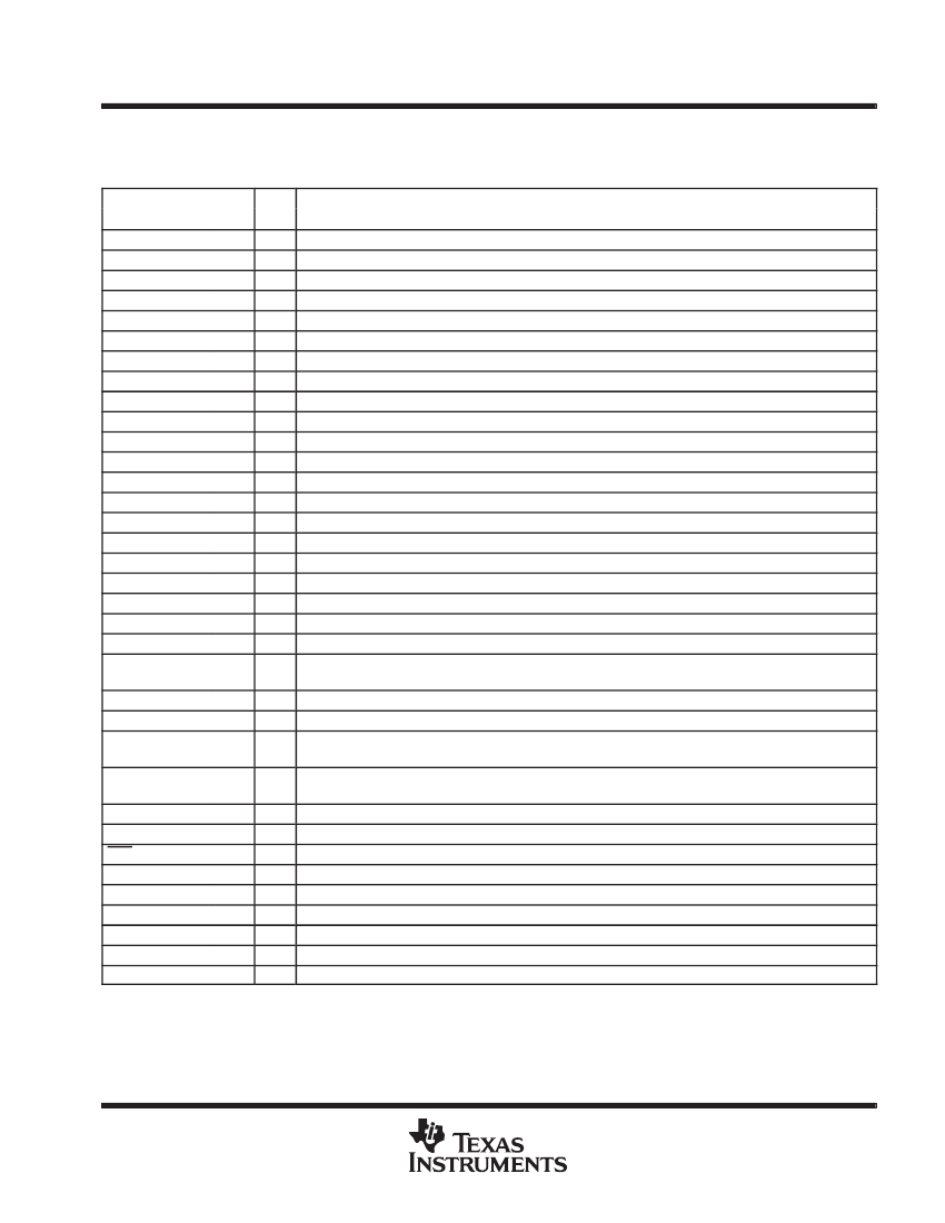
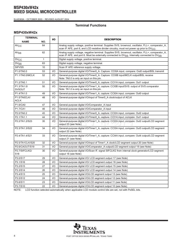
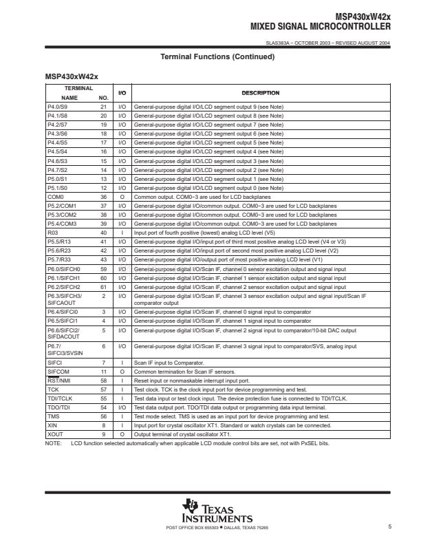
Terminal Functions (Continued)
MSP430xW42x
TERMINAL
NAME
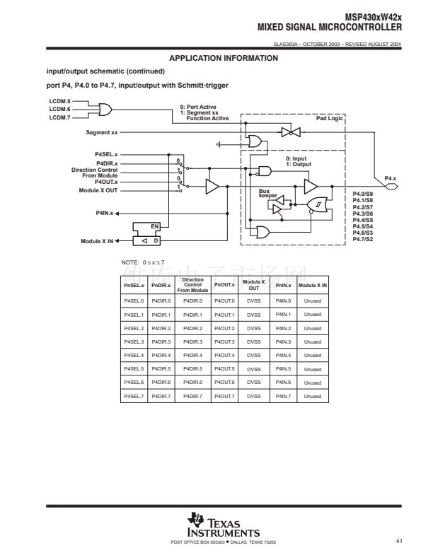
P4.0/S9
P4.1/S8
P4.2/S7
P4.3/S6
P4.4/S5
P4.5/S4
P4.6/S3
P4.7/S2
P5.0/S1
P5.1/S0
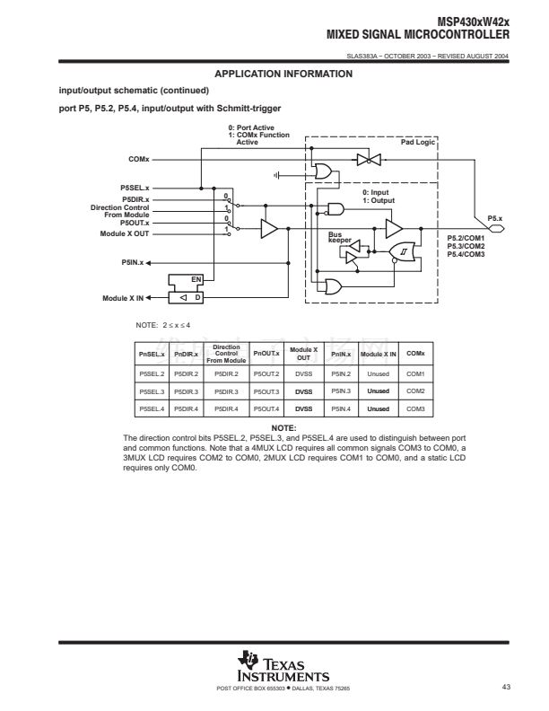
COM0
P5.2/COM1
P5.3/COM2
P5.4/COM3
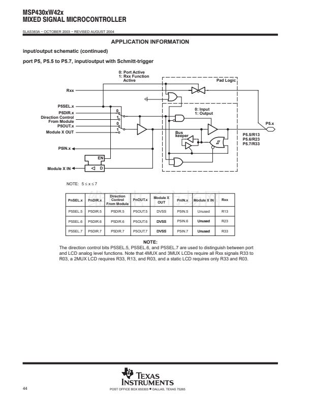
R03
P5.5/R13
P5.6/R23
P5.7/R33
P6.0/SIFCH0
P6.1/SIFCH1
P6.2/SIFCH2
P6.3/SIFCH3/
SIFCAOUT
P6.4/SIFCI0
P6.5/SIFCI1
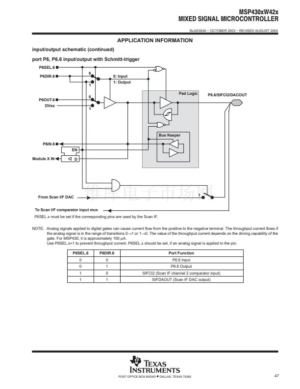
P6.6/SIFCI2/
SIFDACOUT
P6.7/
SIFCI3/SVSIN
SIFCI
SIFCOM
RST/NMI
TCK
TDI/TCLK
TDO/TDI
TMS
XIN
XOUT
NOTE:
NO.
21
20
19
18
17
16
15
14
13
12
36
37
38
39
40
41
42
43
59
60
61
2
3
4
5
6
7
11
58
57
55
54
56
8
9
I/O
I/O
I/O
I/O
I/O
I/O
I/O
I/O
I/O
I/O
I/O
O
I/O
I/O
I/O
I
I/O
I/O
I/O
I/O
I/O
I/O
I/O
I/O
I/O
I/O
I/O
I
O
I
I
I
I/O
I
I
O
DESCRIPTION
General-purpose digital I/O/LCD segment output 9 (see Note)
General-purpose digital I/O/LCD segment output 8 (see Note)
General-purpose digital I/O/LCD segment output 7 (see Note)
General-purpose digital I/O/LCD segment output 6 (see Note)
General-purpose digital I/O/LCD segment output 5 (see Note)
General-purpose digital I/O/LCD segment output 4 (see Note)
General-purpose digital I/O/LCD segment output 3 (see Note)
General-purpose digital I/O/LCD segment output 2 (see Note)
General-purpose digital I/O/LCD segment output 1 (see Note)
General-purpose digital I/O/LCD segment output 0 (see Note)
Common output. COM0鈭? are used for LCD backplanes
General-purpose digital I/O/common output. COM0鈭? are used for LCD backplanes
General-purpose digital I/O/common output. COM0鈭? are used for LCD backplanes
General-purpose digital I/O/common output. COM0鈭? are used for LCD backplanes
Input port of fourth positive (lowest) analog LCD level (V5)
General-purpose digital I/O/input port of third most positive analog LCD level (V4 or V3)
General-purpose digital I/O/input port of second most positive analog LCD level (V2)
General-purpose digital I/O/output port of most positive analog LCD level (V1)
General-purpose digital I/O/Scan IF, channel 0 sensor excitation output and signal input
General-purpose digital I/O/Scan IF, channel 1 sensor excitation output and signal input
General-purpose digital I/O/Scan IF, channel 2 sensor excitation output and signal input
General-purpose digital I/O/Scan IF, channel 3 sensor excitation output and signal input/Scan IF
comparator output
General-purpose digital I/O/Scan IF, channel 0 signal input to comparator
General-purpose digital I/O/Scan IF, channel 1 signal input to comparator
General-purpose digital I/O/Scan IF, channel 2 signal input to comparator/10-bit DAC output
General-purpose digital I/O/Scan IF, channel 3 signal input to comparator/SVS, analog input
Scan IF input to Comparator.
Common termination for Scan IF sensors.
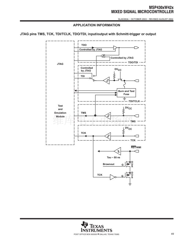
Reset input or nonmaskable interrupt input port.
Test clock. TCK is the clock input port for device programming and test.
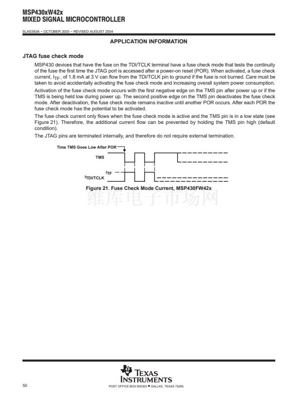
Test data input or test clock input. The device protection fuse is connected to TDI/TCLK.
Test data output port. TDO/TDI data output or programming data input terminal.
Test mode select. TMS is used as an input port for device programming and test.
Input port for crystal oscillator XT1. Standard or watch crystals can be connected.
Output terminal of crystal oscillator XT1.
LCD function selected automatically when applicable LCD module control bits are set, not with PxSEL bits.
POST OFFICE BOX 655303
鈥?/div>
DALLAS, TEXAS 75265
5


 1
1
 2
2
 3
3
 4
4
 5
5
 6
6
 7
7
 8
8
 9
9
 10
10
 11
11
 12
12
 13
13
 14
14
 15
15
 16
16
 17
17
 18
18
 19
19
 20
20
 21
21
 22
22
 23
23
 24
24
 25
25
 26
26
 27
27
 28
28
 29
29
 30
30
 31
31
 32
32
 33
33
 34
34
 35
35
 36
36
 37
37
 38
38
 39
39
 40
40
 41
41
 42
42
 43
43
 44
44
 45
45
 46
46
 47
47
 48
48
 49
49
 50
50
 51
51
 52
52
 53
53
