256-Mbit J3 (x8/x16)
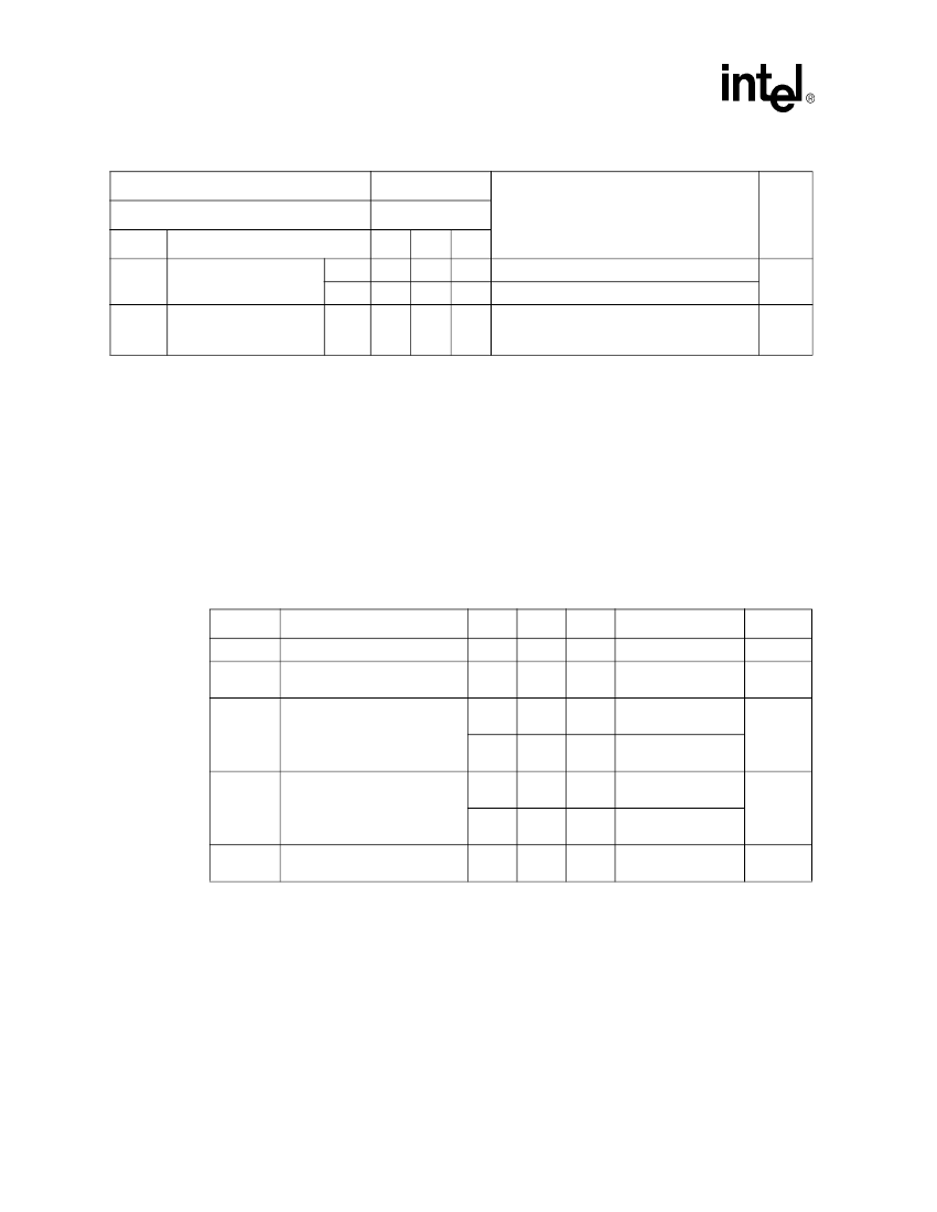
Table 6.
DC Current Characteristics (Sheet 2 of 2)
VCCQ
VCC
2.7 - 3.6V
2.7 - 3.6V
Typ
35
40
Max
70
80
10
Unit
mA
mA
mA
CMOS Inputs, V
PEN
= V
CC
TTL Inputs, V
PEN
= V
CC
Device is enabled (see
Table 13)
1,5
1,4
Test Conditions
Notes
Symbol
I
CCE
I
CCWS
I
CCES
Parameter
V
CC
Block Erase or Clear
Block Lock-Bits Current
V
CC
Program Suspend or
Block Erase Suspend
Current
NOTES:
1. All currents are in RMS unless otherwise noted. These currents are valid for all product versions (packages and
speeds). Contact Intel鈥檚 Application Support Hotline or your local sales office for information about typical
specifications.
2. Includes STS.
3. CMOS inputs are either V
CC
卤 0.2 V or GND 卤 0.2 V. TTL inputs are either V
IL
or V
IH
.
4. Sampled, not 100% tested.
5. I
CCWS
and I
CCES
are specified with the device selected. If the device is read or written while in erase suspend
mode, the device鈥檚 current draw is I
CCR
and I
CCWS
6.2
Table 7.
DC Voltage Characteristics
DC Voltage Characteristics
Symbol
V
IL
V
IH
Parameter
Input Low Voltage
Input High Voltage
Min
鈥?.5
2.0
Max
0.8
V
CCQ
+ 0.5
0.4
V
OL
Output Low Voltage
0.2
0.85
脳
V
CCQ
V
CCQ
鈥?/div>
0.2
V
PEN
Lockout during Program,
Erase and Lock-Bit Operations
2.2
V
V
V
V
Unit
V
V
V
V
CCQ
= V
CCQ
Min
I
OL
= 2 mA
V
CCQ
= V
CCQ
Min
I
OL
= 100 碌A
V
CCQ
= V
CCQ
Min
I
OH
= 鈥?.5 mA
V
CCQ
= V
CCQ
Min
I
OH
= 鈥?00 碌A
2,3,4,7
Test Conditions
Notes
2, 6
2,6
1,2
V
OH
Output High Voltage
1,2
V
PENLK
20
Datasheet
