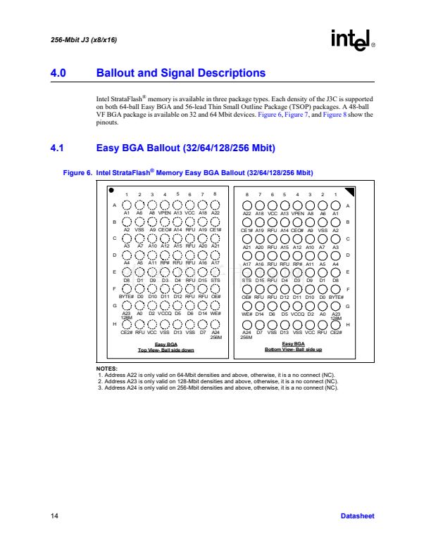
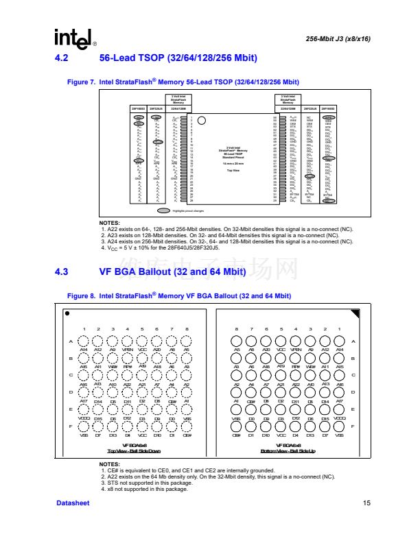
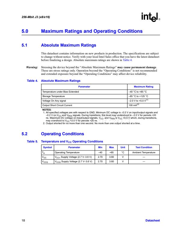
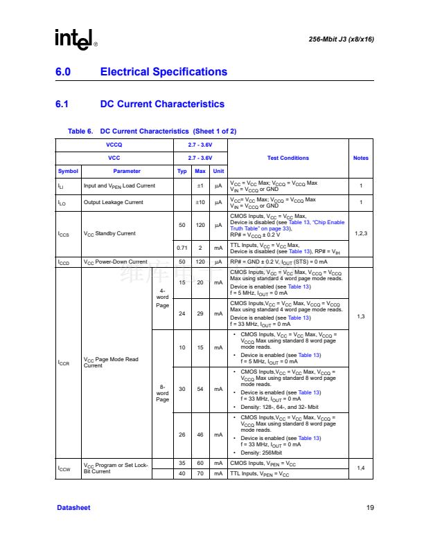
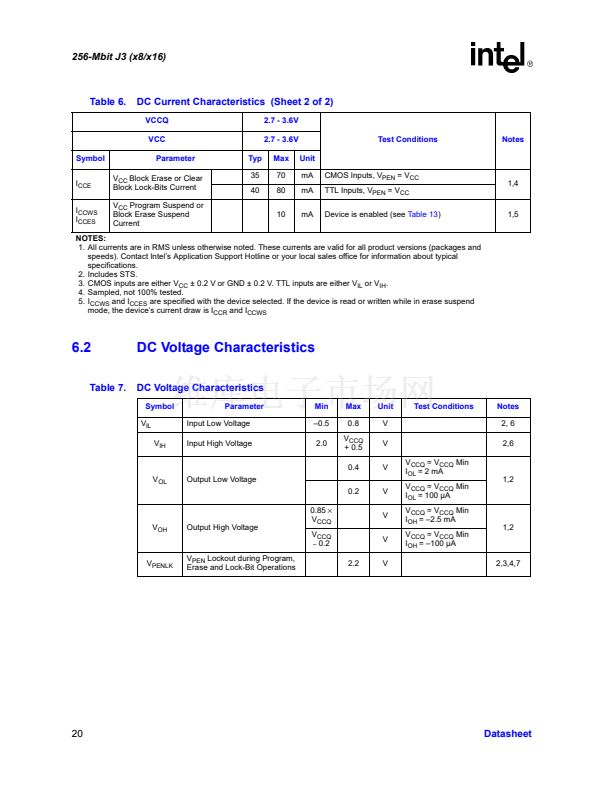
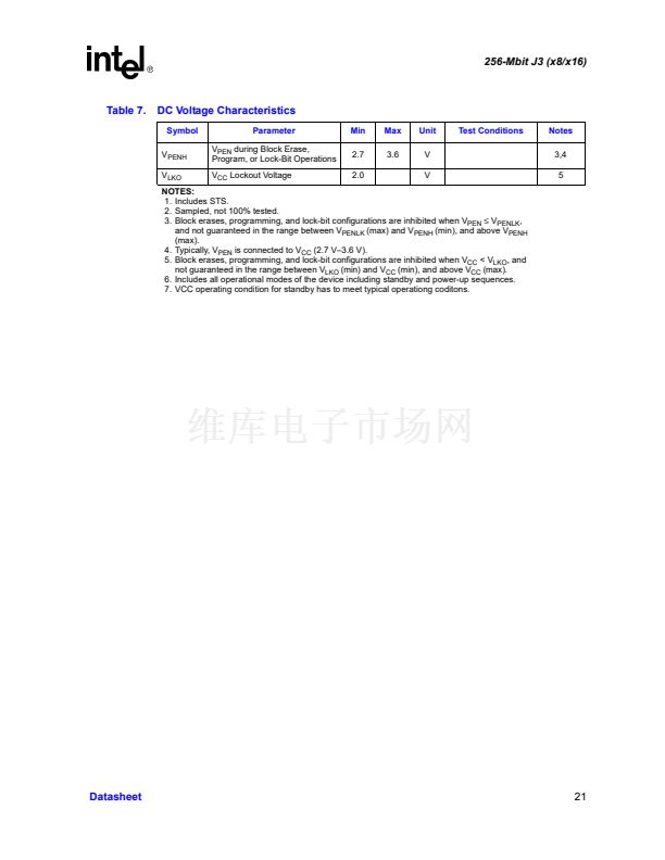
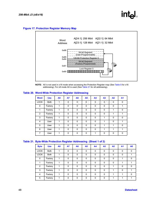
256-Mbit J3 (x8/x16)
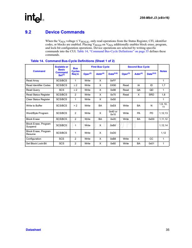
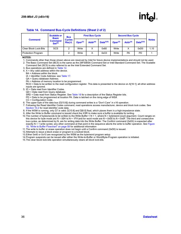
9.0
Bus Operations
This section provides an overview of device bus operations. The on-chip Write State Machine
(WSM) manages all erase and program algorithms. The system CPU provides control of all in-
system read, write, and erase operations of the device via the system bus.
Device commands are written to the CUI to control all of the flash memory device鈥檚 operations.
The CUI does not occupy an addressable memory location; it鈥檚 the mechanism through which the
flash device is controlled.
9.1
Bus Operations Overview
The local CPU reads and writes flash memory in-system. All bus cycles to or from the flash
memory conform to standard microprocessor bus cycles.
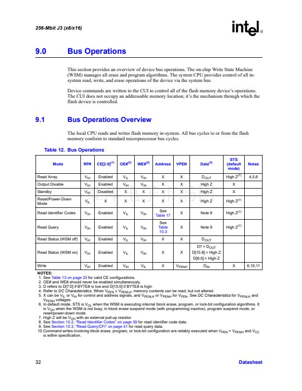
Table 12. Bus Operations
Mode
Read Array
Output Disable
Standby
Reset/Power-Down
Mode
Read Identifier Codes
RP#
V
IH
V
IH
V
IH
V
IL
V
IH
V
IH
V
IH
V
IH
V
IH
CE[2:0]
(1)
Enabled
Enabled
Disabled
X
Enabled
OE#
(2)
V
IL
V
IH
X
X
V
IL
V
IL
V
IL
V
IL
V
IH
WE#
(2)
V
IH
V
IH
X
X
V
IH
V
IH
V
IH
V
IH
V
IL
Address
X
X
X
X
See
Table 17
See
Table
10.3
X
X
X
VPEN
X
X
X
X
X
Data
(3)
D
OUT
High Z
High Z
High Z
Note 8
STS
(default
mode)
High Z
(7)
X
X
High Z
(7)
High Z
(7)
High Z
(7)
Notes
4,5,6
Read Query
Read Status (WSM off)
Read Status (WSM on)
Write
Enabled
Enabled
Enabled
Enabled
X
X
X
V
PENH
Note 9
D
OUT
D7 = D
OUT
D[15:8] = High Z
D[6:0] = High Z
D
IN
X
6,10,11
NOTES:
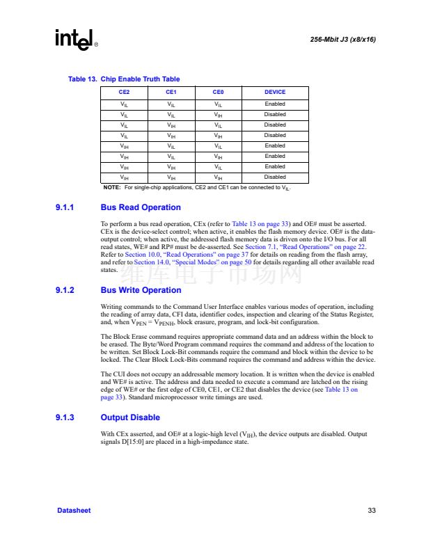
1. See
Table 13 on page 33
for valid CE configurations.
2. OE# and WE# should never be enabled simultaneously.
3. D refers to D[7:0] if BYTE# is low and D[15:0] if BYTE# is high.
4. Refer to
DC Characteristics.
When V
PEN
鈮?/div>
V
PENLK
, memory contents can be read, but not altered.
5. X can be V
IL
or V
IH
for control and address signals, and V
PENLK
or V
PENH
for V
PEN
. See
DC Characteristics
for V
PENLK
and
V
PENH
voltages.
6. In default mode, STS is V
OL
when the WSM is executing internal block erase, program, or lock-bit configuration algorithms. It
is V
OH
when the WSM is not busy, in block erase suspend mode (with programming inactive), program suspend mode, or
reset/power-down mode.
7. High Z will be V
OH
with an external pull-up resistor.
8. See
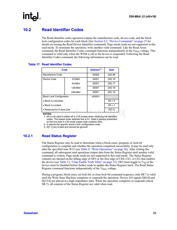
Section 10.2, 鈥淩ead Identifier Codes鈥?on page 39
for read identifier code data.
9. See
Section 10.3, 鈥淩ead Query/CFI鈥?on page 41
for read query data.
10.Command writes involving block erase, program, or lock-bit configuration are reliably executed when V
PEN
= V
PENH
and V
CC
is within specification.
32
Datasheet


 1
1
 2
2
 3
3
 4
4
 5
5
 6
6
 7
7
 8
8
 9
9
 10
10
 11
11
 12
12
 13
13
 14
14
 15
15
 16
16
 17
17
 18
18
 19
19
 20
20
 21
21
 22
22
 23
23
 24
24
 25
25
 26
26
 27
27
 28
28
 29
29
 30
30
 31
31
 32
32
 33
33
 34
34
 35
35
 36
36
 37
37
 38
38
 39
39
 40
40
 41
41
 42
42
 43
43
 44
44
 45
45
 46
46
 47
47
 48
48
 49
49
 50
50
 51
51
 52
52
 53
53
 54
54
 55
55
 56
56
 57
57
 58
58
 59
59
 60
60
 61
61
 62
62
 63
63
 64
64
 65
65
 66
66
 67
67
 68
68
 69
69
 70
70
 71
71
 72
72
