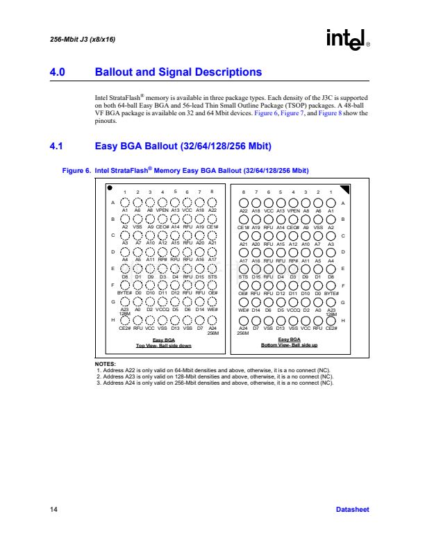
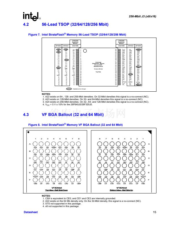
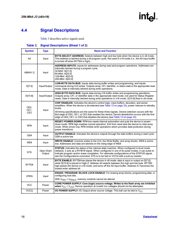
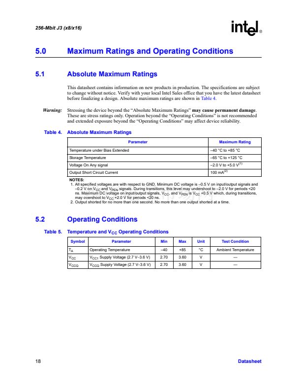
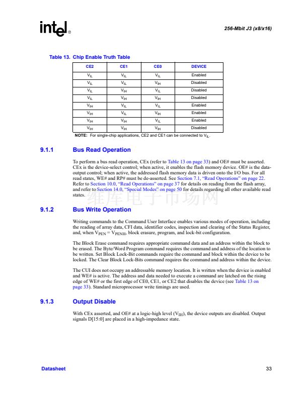
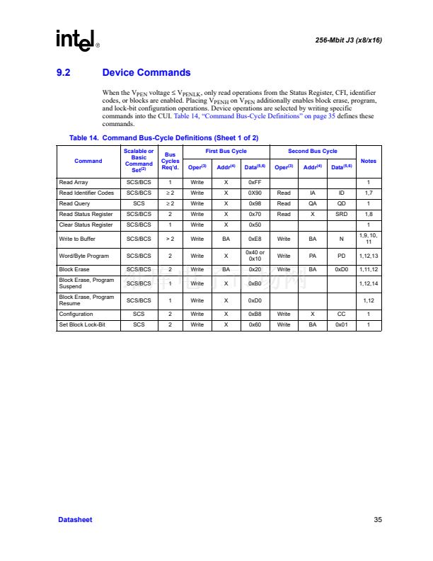
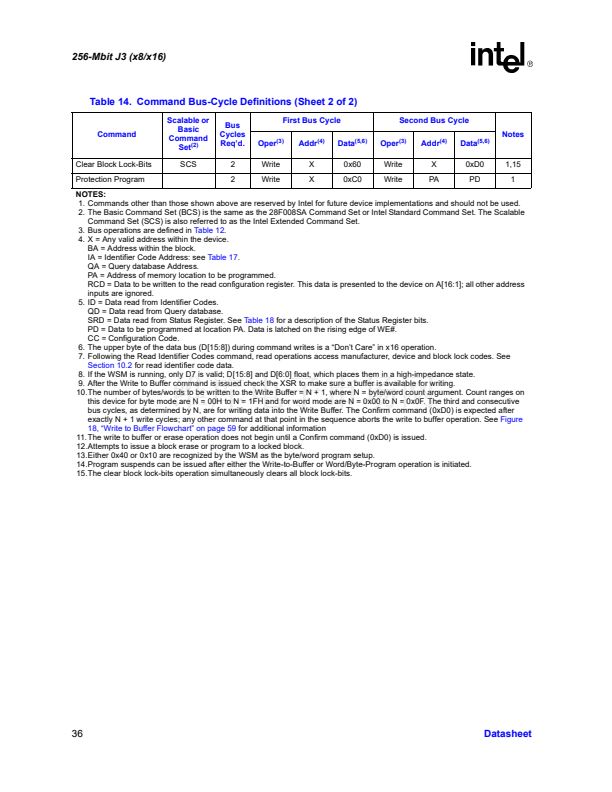
鈮?/div>
V
PENLK
, only read operations from the Status Register, CFI, identifier
codes, or blocks are enabled. Placing V
PENH
on V
PEN
additionally enables block erase, program,
and lock-bit configuration operations. Device operations are selected by writing specific
commands into the CUI.
Table 14, 鈥淐ommand Bus-Cycle Definitions鈥?on page 35
defines these
commands.
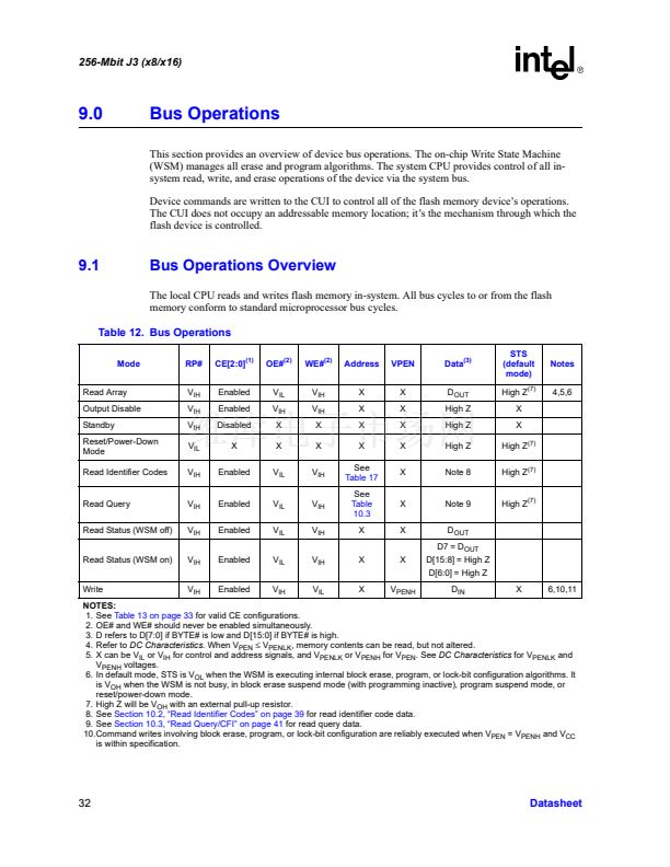
Table 14. Command Bus-Cycle Definitions (Sheet 1 of 2)
Command
Scalable or
Basic
Command
Set
(2)
SCS/BCS
SCS/BCS
SCS
SCS/BCS
SCS/BCS
SCS/BCS
SCS/BCS
SCS/BCS
SCS/BCS
SCS/BCS
SCS
SCS
Bus
Cycles
Req鈥檇.
1
鈮?/div>
2
鈮?/div>
2
2
1
>2
2
2
1
1
2
2
First Bus Cycle
Oper
(3)
Second Bus Cycle
Notes
(5,6)
Addr
X
X
X
X
X
BA
X
BA
X
X
X
X
(4)
Data
Oper
(3)
Addr
(4)
Data
(5,6)
Read Array
Read Identifier Codes
Read Query
Read Status Register
Clear Status Register
Write to Buffer
Word/Byte Program
Block Erase
Block Erase, Program
Suspend
Block Erase, Program
Resume
Configuration
Set Block Lock-Bit
Write
Write
Write
Write
Write
Write
Write
Write
Write
Write
Write
Write
0xFF
0X90
0x98
0x70
0x50
0xE8
0x40 or
0x10
0x20
0xB0
0xD0
0xB8
0x60
Write
Write
X
BA
CC
0x01
Write
Write
Write
BA
PA
BA
N
PD
0xD0
Read
Read
Read
IA
QA
X
ID
QD
SRD
1
1,7
1
1,8
1
1,9, 10,
11
1,12,13
1,11,12
1,12,14
1,12
1
1
Datasheet
35


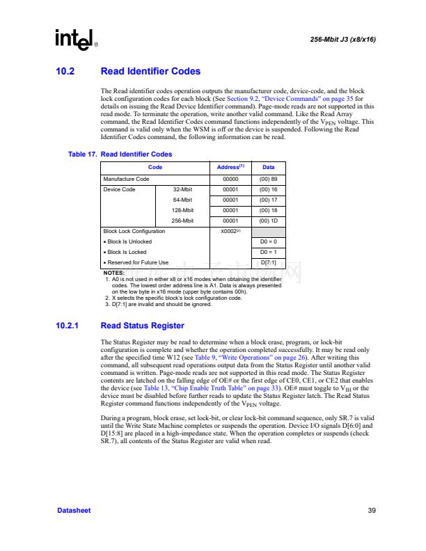
 1
1
 2
2
 3
3
 4
4
 5
5
 6
6
 7
7
 8
8
 9
9
 10
10
 11
11
 12
12
 13
13
 14
14
 15
15
 16
16
 17
17
 18
18
 19
19
 20
20
 21
21
 22
22
 23
23
 24
24
 25
25
 26
26
 27
27
 28
28
 29
29
 30
30
 31
31
 32
32
 33
33
 34
34
 35
35
 36
36
 37
37
 38
38
 39
39
 40
40
 41
41
 42
42
 43
43
 44
44
 45
45
 46
46
 47
47
 48
48
 49
49
 50
50
 51
51
 52
52
 53
53
 54
54
 55
55
 56
56
 57
57
 58
58
 59
59
 60
60
 61
61
 62
62
 63
63
 64
64
 65
65
 66
66
 67
67
 68
68
 69
69
 70
70
 71
71
 72
72
