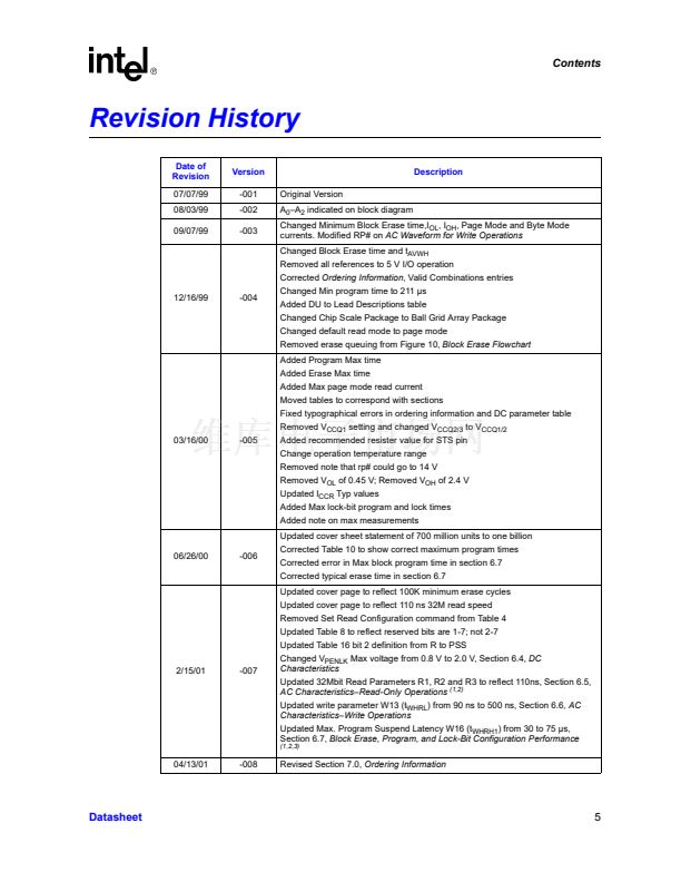
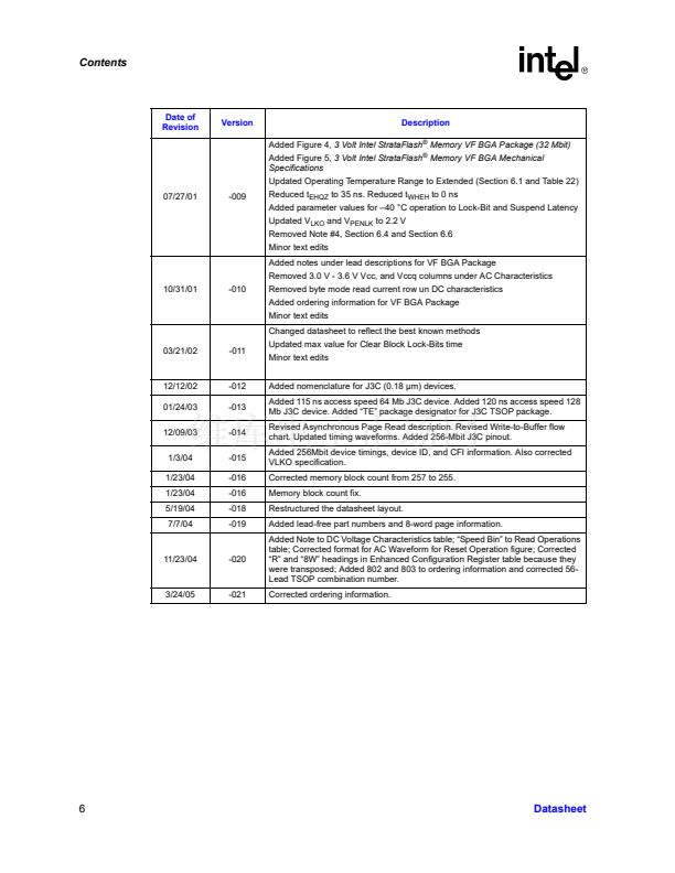
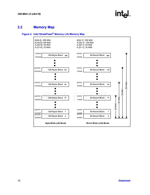
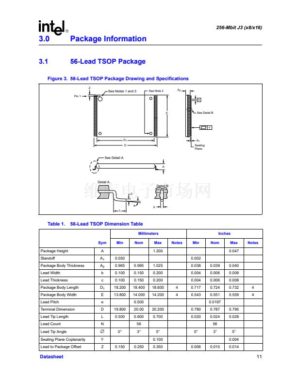
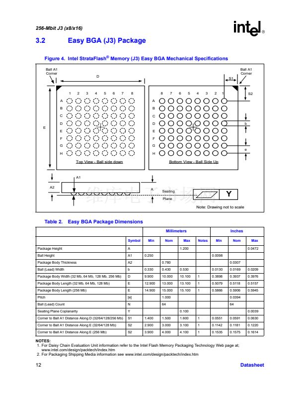
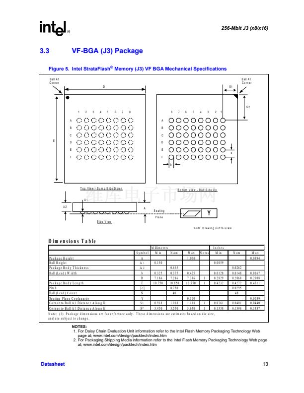
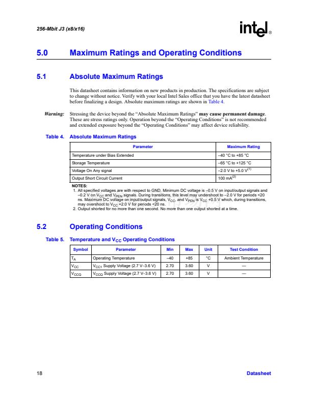
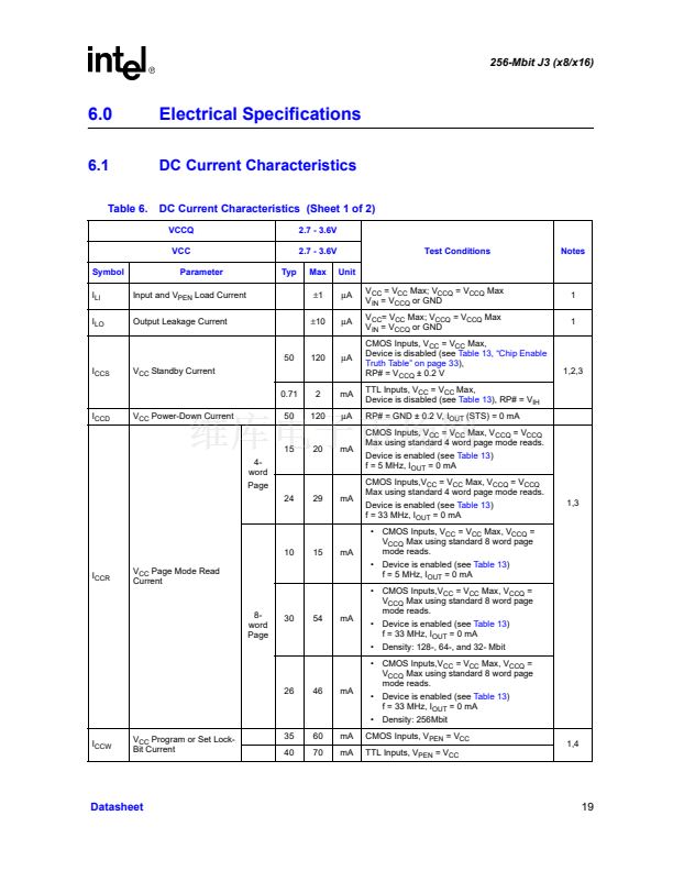
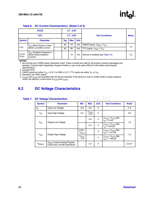
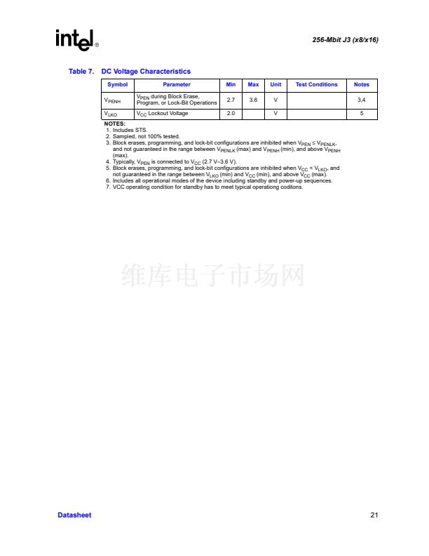
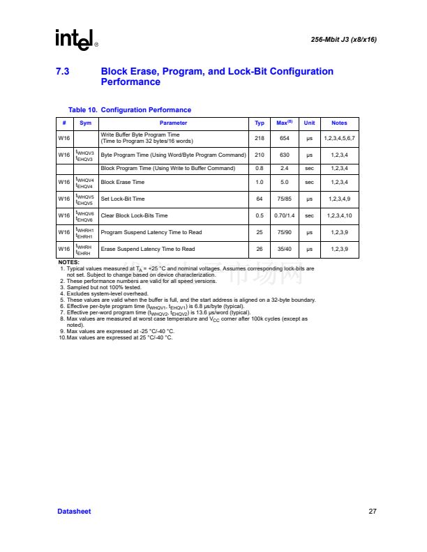
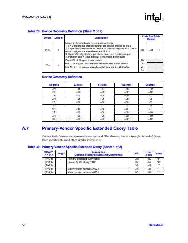
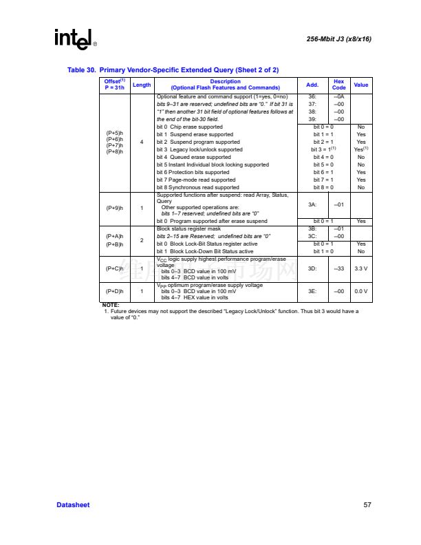
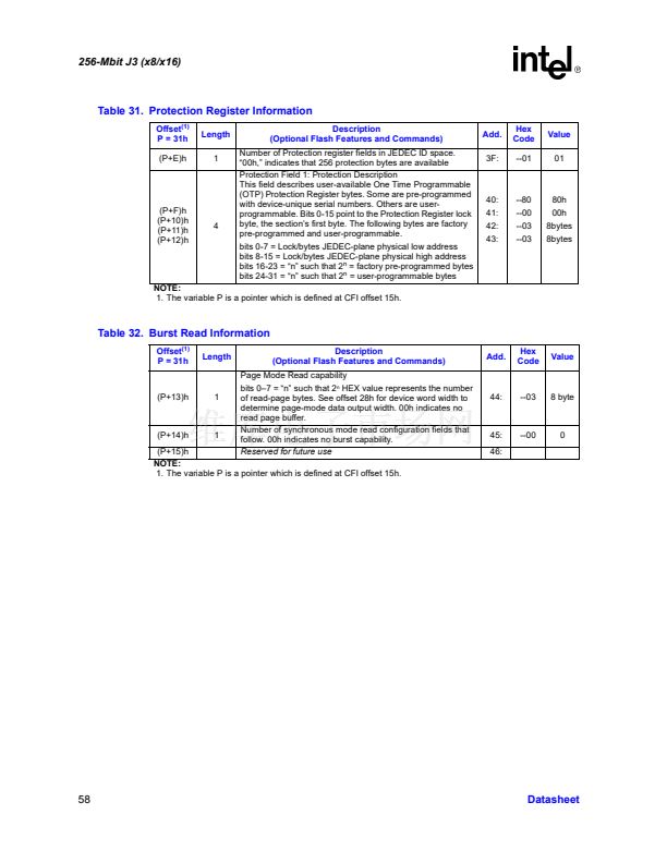
256-Mbit J3 (x8/x16)
Table 14. Command Bus-Cycle Definitions (Sheet 2 of 2)
Command
Scalable or
Basic
Command
Set
(2)
SCS
Bus
Cycles
Req鈥檇.
2
2
First Bus Cycle
Oper
(3)
Write
Write
Addr
(4)
X
X
Data
(5,6)
0x60
0xC0
Second Bus Cycle
Notes
Oper
(3)
Write
Write
Addr
(4)
X
PA
Data
(5,6)
0xD0
PD
1,15
1
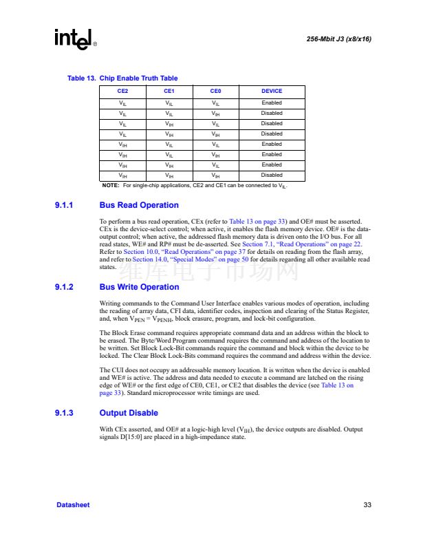
Clear Block Lock-Bits
Protection Program
NOTES:
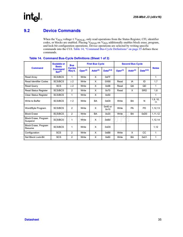
1. Commands other than those shown above are reserved by Intel for future device implementations and should not be used.
2. The Basic Command Set (BCS) is the same as the 28F008SA Command Set or Intel Standard Command Set. The Scalable
Command Set (SCS) is also referred to as the Intel Extended Command Set.
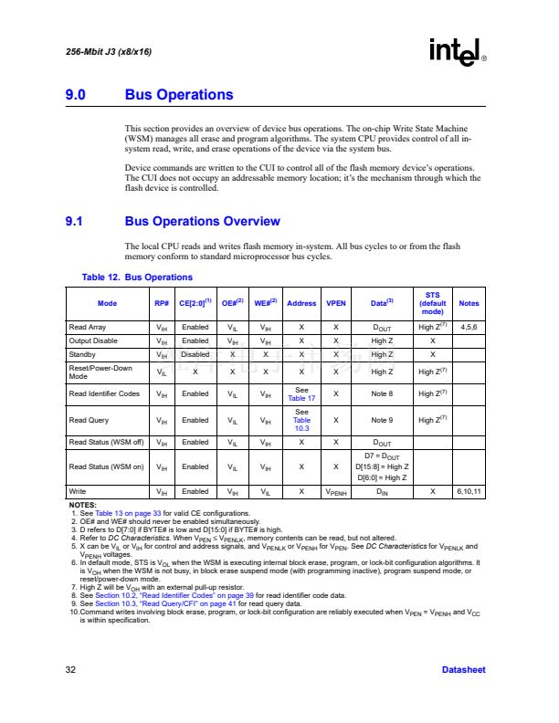
3. Bus operations are defined in
Table 12.
4. X = Any valid address within the device.
BA = Address within the block.
IA = Identifier Code Address: see
Table 17.
QA = Query database Address.
PA = Address of memory location to be programmed.
RCD = Data to be written to the read configuration register. This data is presented to the device on A[16:1]; all other address
inputs are ignored.
5. ID = Data read from Identifier Codes.
QD = Data read from Query database.
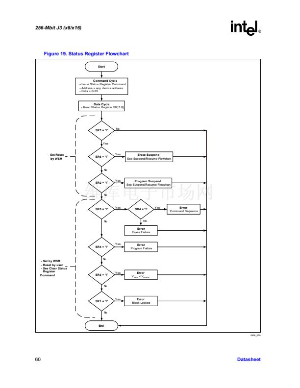
SRD = Data read from Status Register. See
Table 18
for a description of the Status Register bits.
PD = Data to be programmed at location PA. Data is latched on the rising edge of WE#.
CC = Configuration Code.
6. The upper byte of the data bus (D[15:8]) during command writes is a 鈥淒on鈥檛 Care鈥?in x16 operation.
7. Following the Read Identifier Codes command, read operations access manufacturer, device and block lock codes. See
Section 10.2
for read identifier code data.
8. If the WSM is running, only D7 is valid; D[15:8] and D[6:0] float, which places them in a high-impedance state.
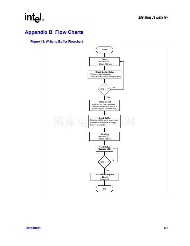
9. After the Write to Buffer command is issued check the XSR to make sure a buffer is available for writing.
10.The number of bytes/words to be written to the Write Buffer = N + 1, where N = byte/word count argument. Count ranges on
this device for byte mode are N = 00H to N = 1FH and for word mode are N = 0x00 to N = 0x0F. The third and consecutive
bus cycles, as determined by N, are for writing data into the Write Buffer. The Confirm command (0xD0) is expected after
exactly N + 1 write cycles; any other command at that point in the sequence aborts the write to buffer operation. See
Figure
18, 鈥淲rite to Buffer Flowchart鈥?on page 59
for additional information
11.The write to buffer or erase operation does not begin until a Confirm command (0xD0) is issued.
12.Attempts to issue a block erase or program to a locked block.
13.Either 0x40 or 0x10 are recognized by the WSM as the byte/word program setup.
14.Program suspends can be issued after either the Write-to-Buffer or Word/Byte-Program operation is initiated.
15.The clear block lock-bits operation simultaneously clears all block lock-bits.
36
Datasheet


 1
1
 2
2
 3
3
 4
4
 5
5
 6
6
 7
7
 8
8
 9
9
 10
10
 11
11
 12
12
 13
13
 14
14
 15
15
 16
16
 17
17
 18
18
 19
19
 20
20
 21
21
 22
22
 23
23
 24
24
 25
25
 26
26
 27
27
 28
28
 29
29
 30
30
 31
31
 32
32
 33
33
 34
34
 35
35
 36
36
 37
37
 38
38
 39
39
 40
40
 41
41
 42
42
 43
43
 44
44
 45
45
 46
46
 47
47
 48
48
 49
49
 50
50
 51
51
 52
52
 53
53
 54
54
 55
55
 56
56
 57
57
 58
58
 59
59
 60
60
 61
61
 62
62
 63
63
 64
64
 65
65
 66
66
 67
67
 68
68
 69
69
 70
70
 71
71
 72
72
