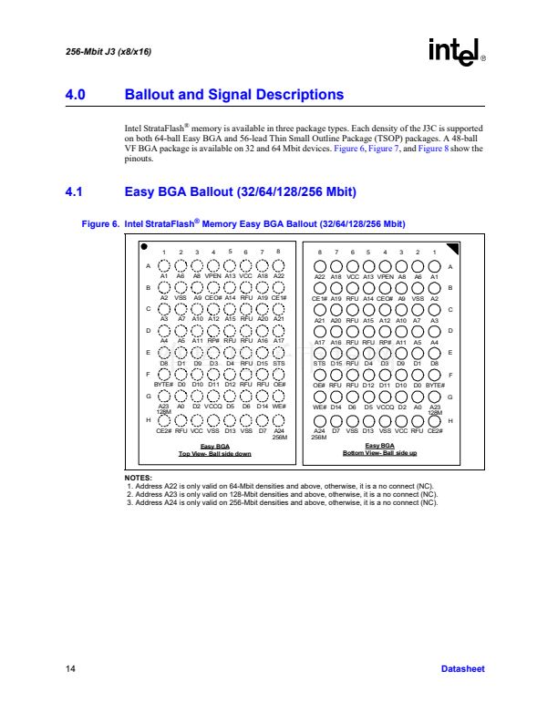
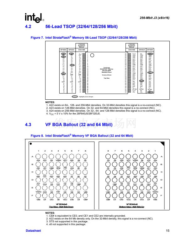
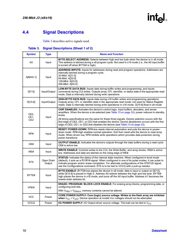
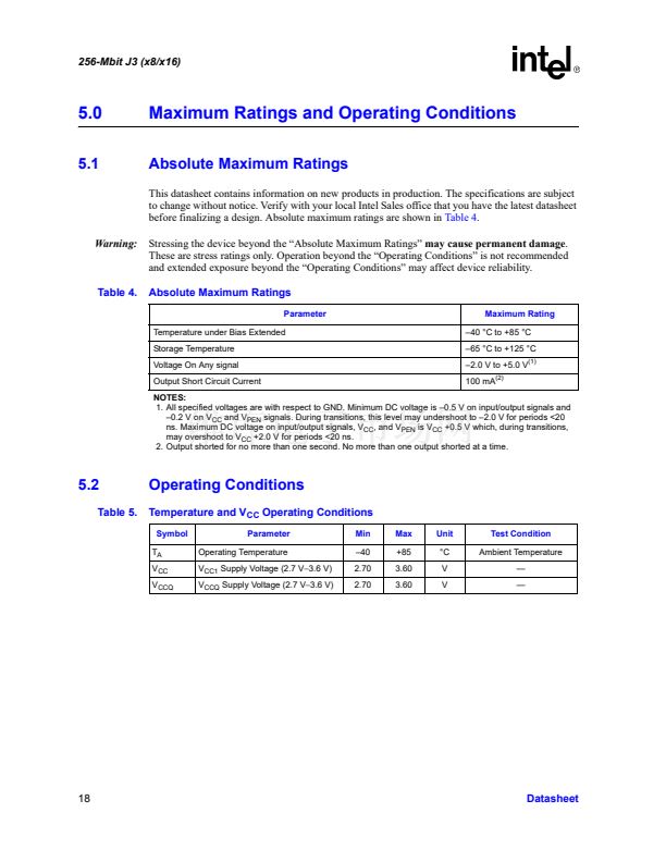
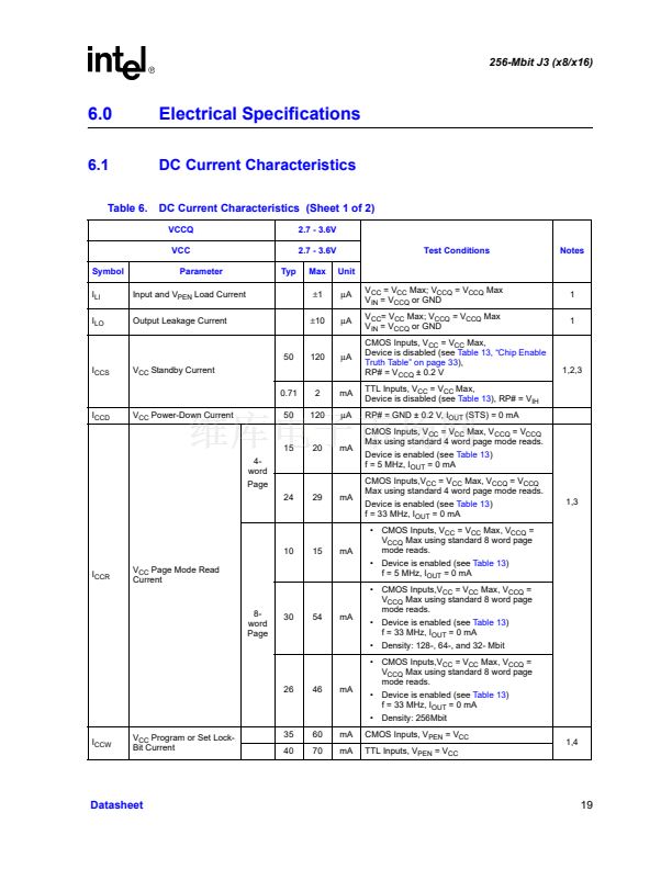
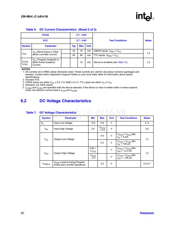
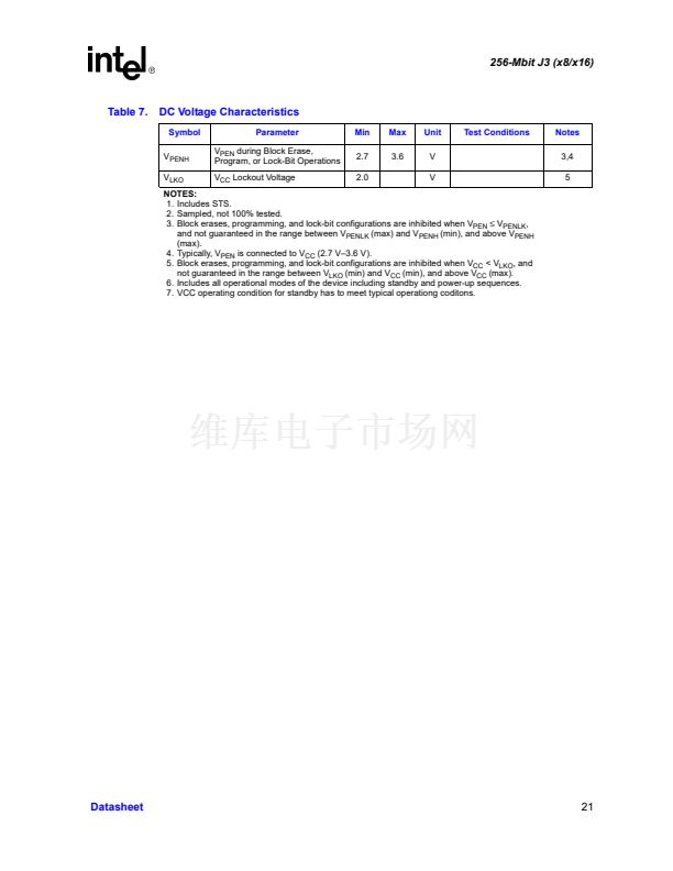
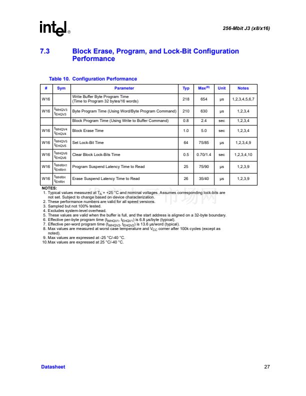
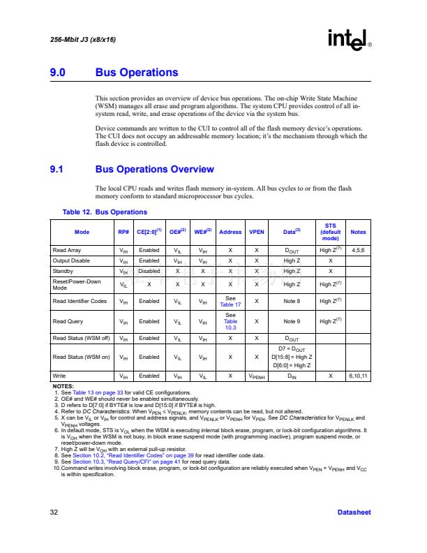
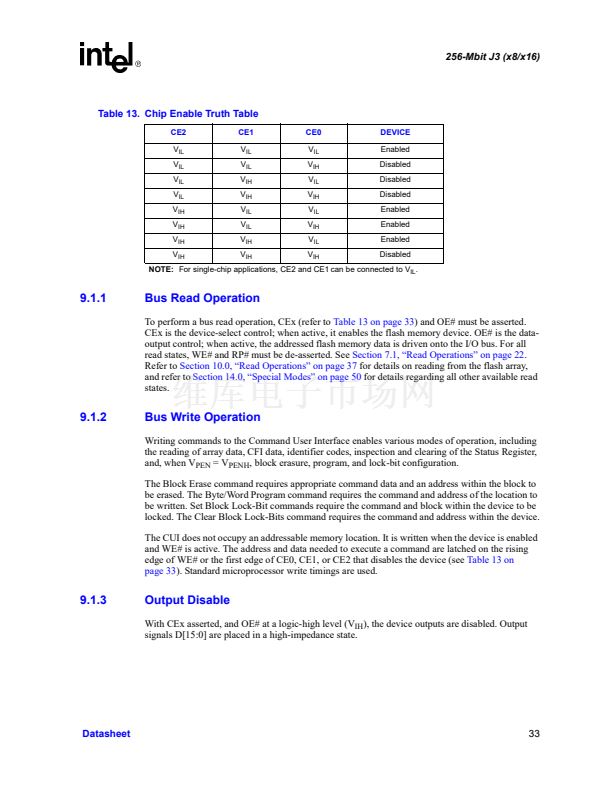
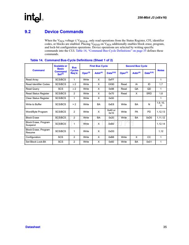
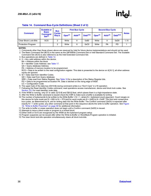
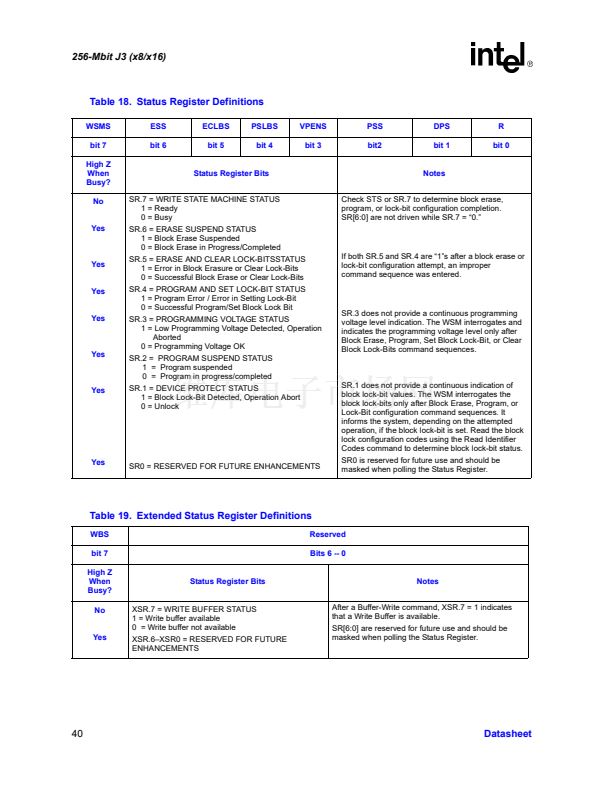
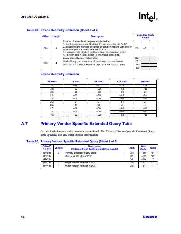
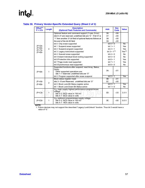
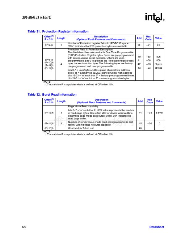
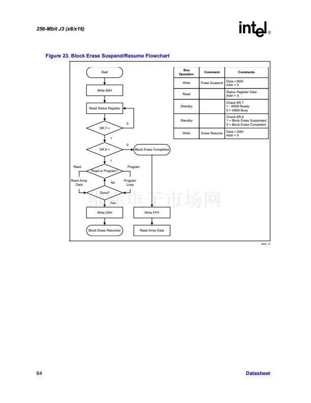
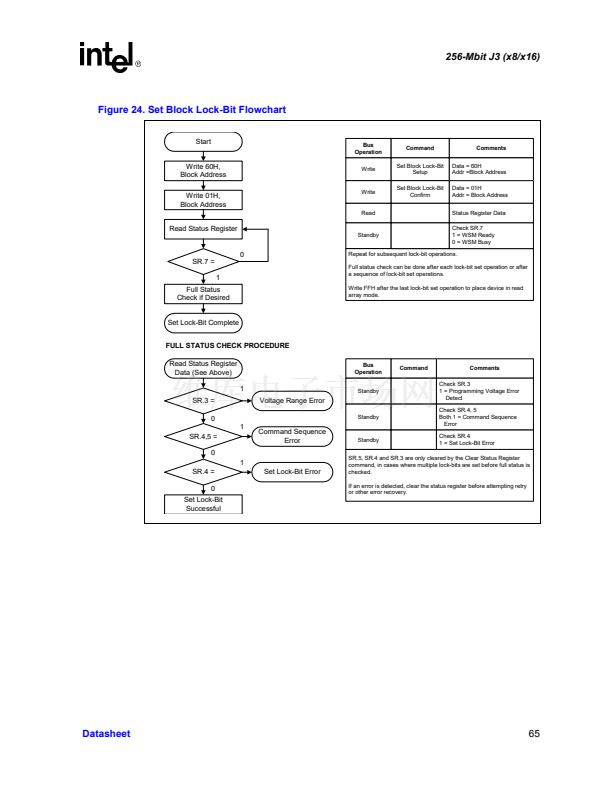
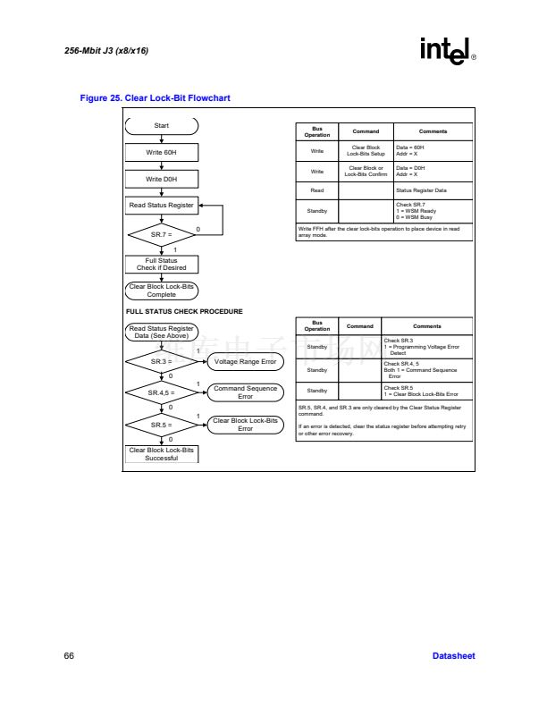
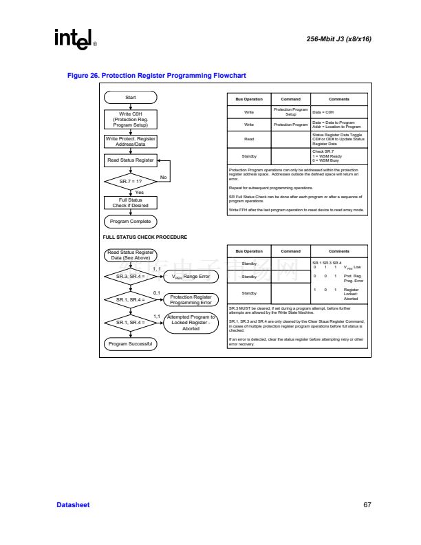
256-Mbit J3 (x8/x16)
11.0
Programming Operations
The device supports two different programming methods: word programming, and write-buffer
programming. Successful programming requires the addressed block to be unlocked. An attempt to
program a locked block will result in the operation aborting, and SR.1 and SR.4 being set,
indicating a programming error. The following sections describe device programming in detail.
11.1
Byte/Word Program
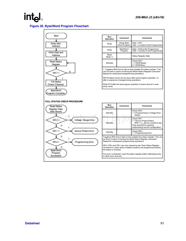
Byte/Word program is executed by a two-cycle command sequence. Byte/Word program setup
(standard 0x40 or alternate 0x10) is written followed by a second write that specifies the address
and data (latched on the rising edge of WE#). The WSM then takes over, controlling the program
and program verify algorithms internally. After the program sequence is written, the device
automatically outputs SRD when read (see
Figure 20, 鈥淏yte/Word Program Flowchart鈥?on
page 61).
The CPU can detect the completion of the program event by analyzing the STS signal or
SR.7.
When program is complete, SR.4 should be checked. If a program error is detected, the Status
Register should be cleared. The internal WSM verify only detects errors for 鈥?鈥漵 that do not
successfully program to 鈥?鈥漵. The CUI remains in Read Status Register mode until it receives
another command.
Reliable byte/word programming can only occur when V
CC
and V
PEN
are valid. If a byte/word
program is attempted while V
PEN
鈮?/div>
V
PENLK
, SR.4 and SR.3 will be set. Successful byte/word
programs require that the corresponding block lock-bit be cleared. If a byte/word program is
attempted when the corresponding block lock-bit is set, SR.1 and SR.4 will be set.
11.2
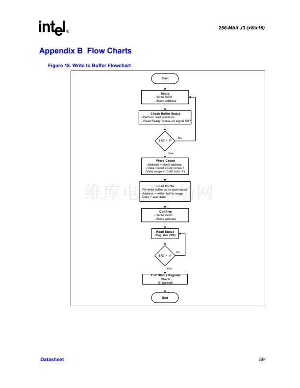
Write to Buffer
To program the flash device, a Write to Buffer command sequence is initiated. A variable number
of bytes, up to the buffer size, can be loaded into the buffer and written to the flash device. First, the
Write to Buffer Setup command is issued along with the Block Address (see
Figure 18, 鈥淲rite to
Buffer Flowchart鈥?on page 59).
At this point, the eXtended Status Register (XSR, see
Table 19)
information is loaded and XSR.7 reverts to 鈥渂uffer available鈥?status. If XSR.7 = 0, the write buffer
is not available. To retry, continue monitoring XSR.7 by issuing the Write to Buffer setup
command with the Block Address until XSR.7 = 1. When XSR.7 transitions to a 鈥?,鈥?the buffer is
ready for loading.
Next, a word/byte count is given to the part with the Block Address. On the next write, a device
start address is given along with the write buffer data. Subsequent writes provide additional device
addresses and data, depending on the count. All subsequent addresses must lie within the start
address plus the count.
Internally, this device programs many flash cells in parallel. Because of this parallel programming,
maximum programming performance and lower power are obtained by aligning the start address at
the beginning of a write buffer boundary (i.e., A[4:0] of the start address = 0).
42
Datasheet


 1
1
 2
2
 3
3
 4
4
 5
5
 6
6
 7
7
 8
8
 9
9
 10
10
 11
11
 12
12
 13
13
 14
14
 15
15
 16
16
 17
17
 18
18
 19
19
 20
20
 21
21
 22
22
 23
23
 24
24
 25
25
 26
26
 27
27
 28
28
 29
29
 30
30
 31
31
 32
32
 33
33
 34
34
 35
35
 36
36
 37
37
 38
38
 39
39
 40
40
 41
41
 42
42
 43
43
 44
44
 45
45
 46
46
 47
47
 48
48
 49
49
 50
50
 51
51
 52
52
 53
53
 54
54
 55
55
 56
56
 57
57
 58
58
 59
59
 60
60
 61
61
 62
62
 63
63
 64
64
 65
65
 66
66
 67
67
 68
68
 69
69
 70
70
 71
71
 72
72
