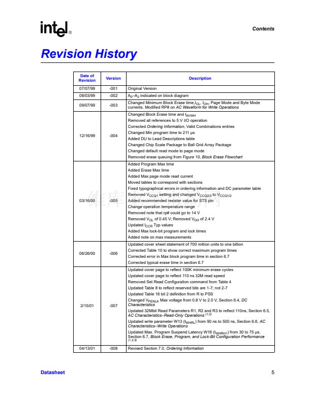
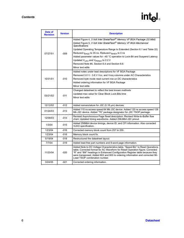
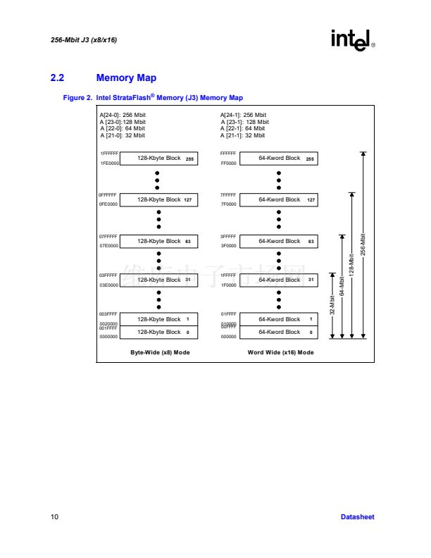
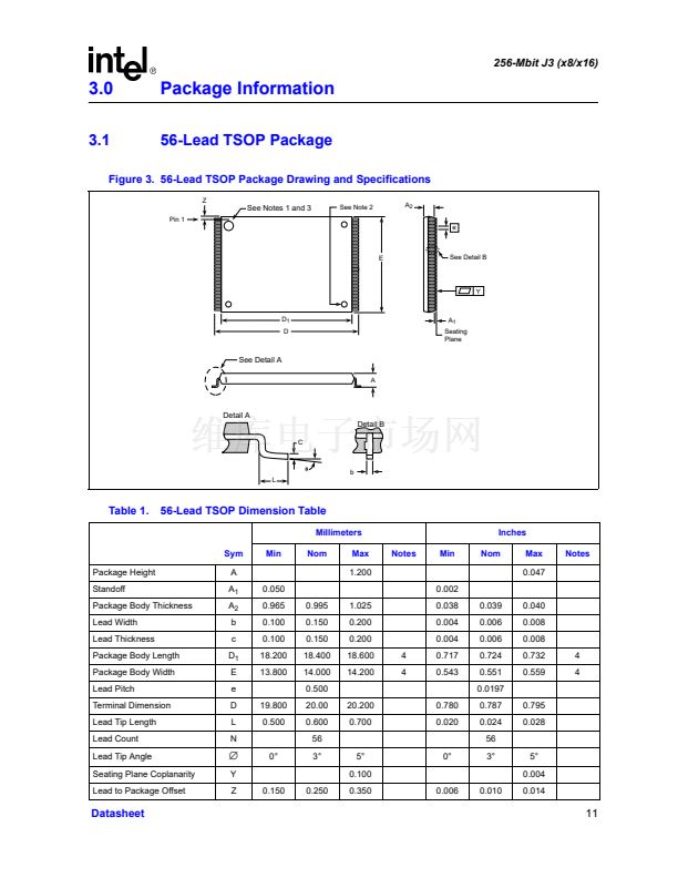
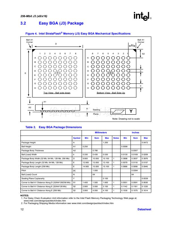
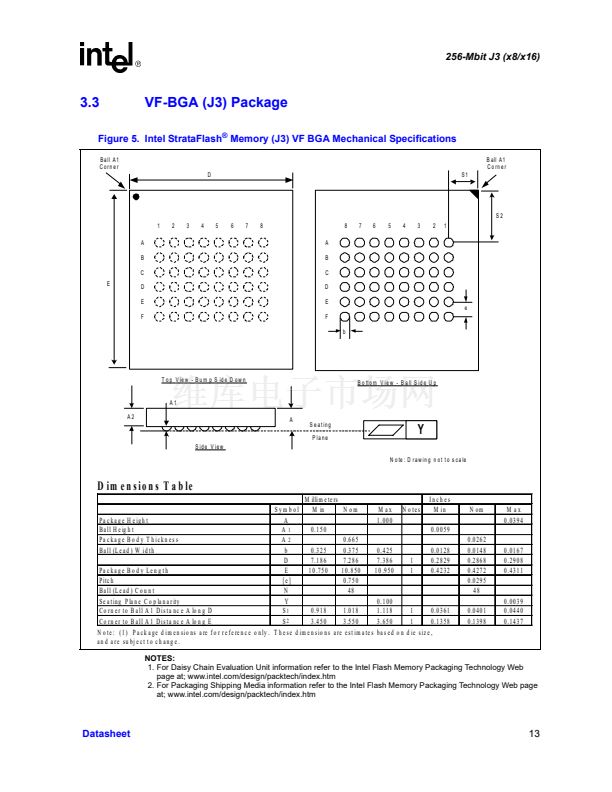
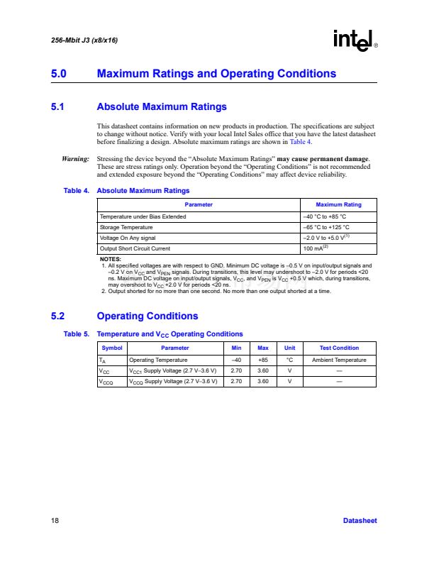
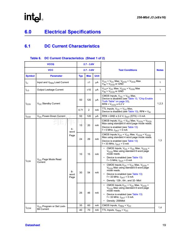
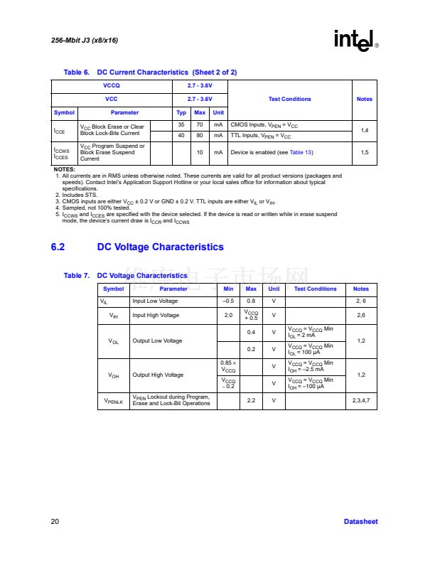
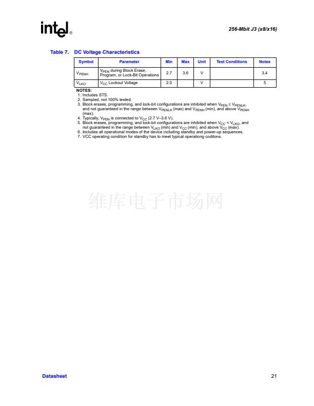
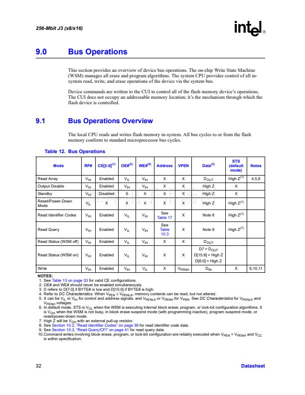
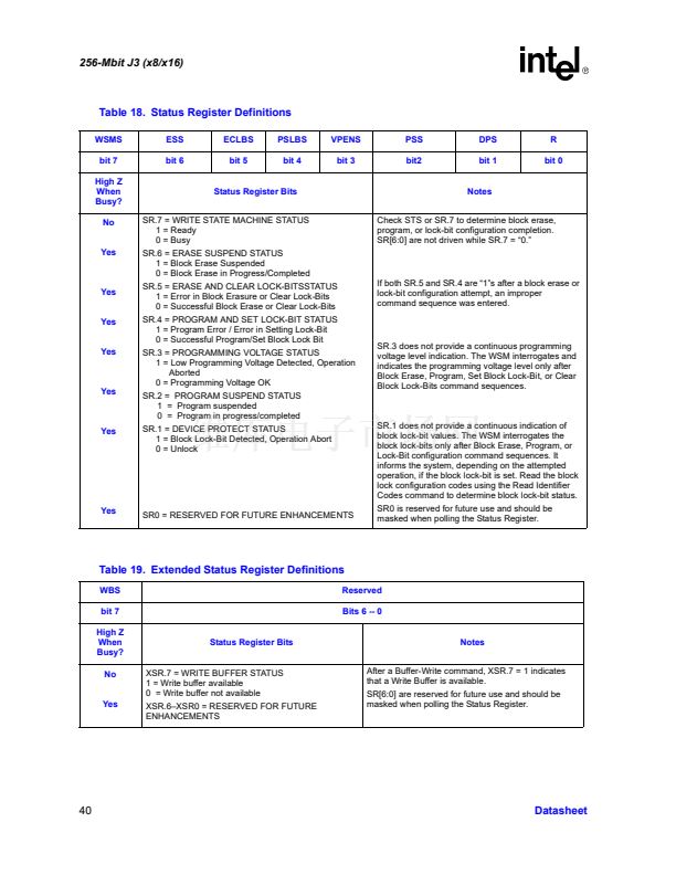
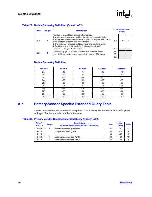
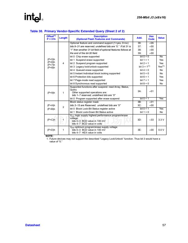
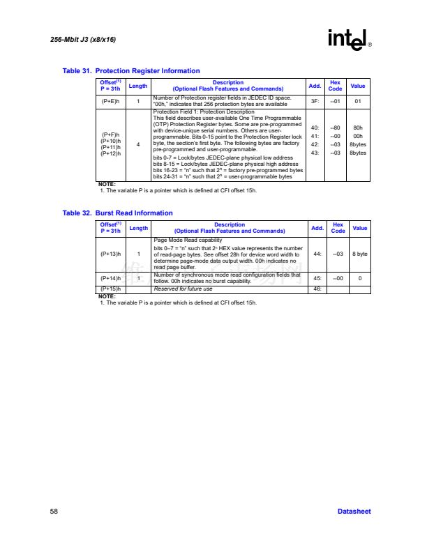
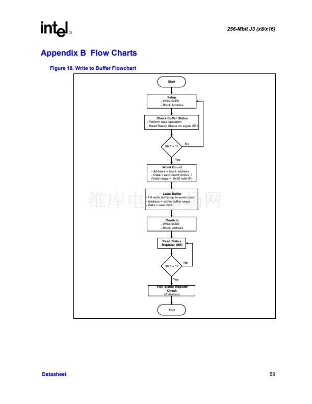
256-Mbit J3 (x8/x16)
12.0
Erase Operations
Flash erasing is performed on a block basis; therefore, only one block can be erased at a time. Once
a block is erased, all bits within that block will read as a logic level one. To determine the status of
a block erase, poll the Status Register and analyze the bits. This following section describes block
erase operations in detail.
12.1
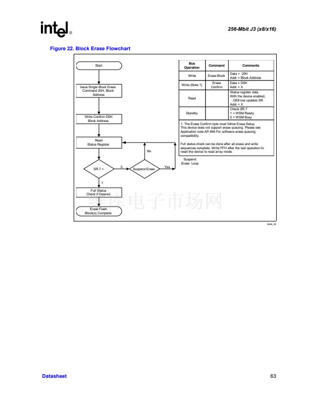
Block Erase
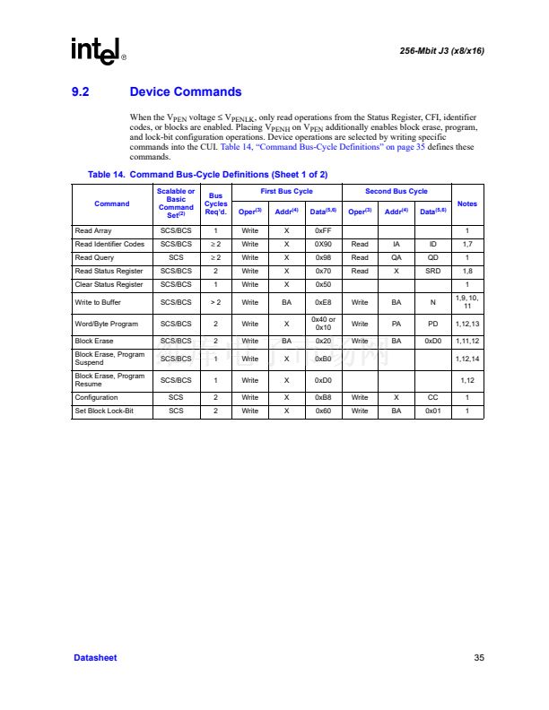
Erase is executed one block at a time and initiated by a two-cycle command. A block erase setup is
first written, followed by an block erase confirm. This command sequence requires an appropriate
address within the block to be erased (erase changes all block data to FFH). Block preconditioning,
erase, and verify are handled internally by the WSM (invisible to the system). After the two-cycle
block erase sequence is written, the device automatically outputs SRD when read (see
Figure 22,
鈥淏lock Erase Flowchart鈥?on page 63).
The CPU can detect block erase completion by analyzing
the output of the STS signal or SR.7. Toggle OE#, CE0, CE1, or CE2 to update the Status Register.
When the block erase is complete, SR.5 should be checked. If a block erase error is detected, the
Status Register should be cleared before system software attempts corrective actions. The CUI
remains in Read Status Register mode until a new command is issued.
This two-step command sequence of setup followed by execution ensures that block contents are
not accidentally erased. An invalid Block Erase command sequence will result in both SR.4 and
SR.5 being set. Also, reliable block erasure can only occur when V
CC
is valid and V
PEN
= V
PENH
.
If block erase is attempted while V
PEN
鈮?/div>
V
PENLK
, SR.3 and SR.5 will be set. Successful block
erase requires that the corresponding block lock-bit be cleared. If block erase is attempted when the
corresponding block lock-bit is set, SR.1 and SR.5 will be set.
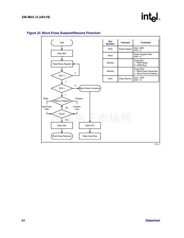
12.2
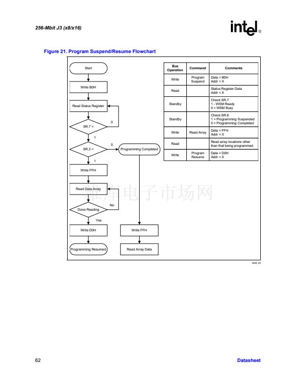
Block Erase Suspend
The Block Erase Suspend command allows block-erase interruption to read or program data in
another block of memory. Once the block erase process starts, writing the Block Erase Suspend
command requests that the WSM suspend the block erase sequence at a predetermined point in the
algorithm. The device outputs SRD when read after the Block Erase Suspend command is written.
Polling SR.7 then SR.6 can determine when the block erase operation has been suspended (both
will be set). In default mode, STS will also transition to V
OH
. Specification t
WHRH
defines the
block erase suspend latency.
At this point, a Read Array command can be written to read data from blocks other than that which
is suspended. A program command sequence can also be issued during erase suspend to program
data in other blocks. During a program operation with block erase suspended, SR.7 will return to
鈥?鈥?and STS output (in default mode) will transition to V
OL
. However, SR.6 will remain 鈥?鈥?to
indicate block erase suspend status. Using the Program Suspend command, a program operation
can also be suspended. Resuming a suspended programming operation by issuing the Program
Resume command allows continuing of the suspended programming operation. To resume the
suspended erase, the user must wait for the programming operation to complete before issuing the
Block Erase Resume command.
44
Datasheet


 1
1
 2
2
 3
3
 4
4
 5
5
 6
6
 7
7
 8
8
 9
9
 10
10
 11
11
 12
12
 13
13
 14
14
 15
15
 16
16
 17
17
 18
18
 19
19
 20
20
 21
21
 22
22
 23
23
 24
24
 25
25
 26
26
 27
27
 28
28
 29
29
 30
30
 31
31
 32
32
 33
33
 34
34
 35
35
 36
36
 37
37
 38
38
 39
39
 40
40
 41
41
 42
42
 43
43
 44
44
 45
45
 46
46
 47
47
 48
48
 49
49
 50
50
 51
51
 52
52
 53
53
 54
54
 55
55
 56
56
 57
57
 58
58
 59
59
 60
60
 61
61
 62
62
 63
63
 64
64
 65
65
 66
66
 67
67
 68
68
 69
69
 70
70
 71
71
 72
72
