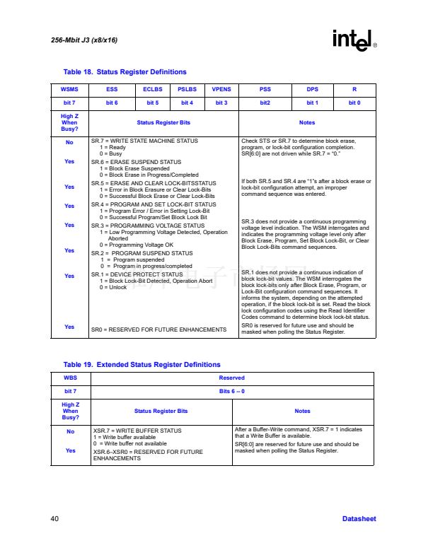
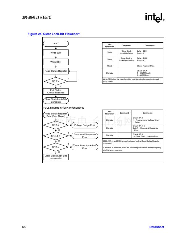
This two-step sequence of setup followed by execution ensures that block lock-bits are not
accidentally cleared. An invalid Clear Block Lock-Bits command sequence will result in SR.4 and
SR.5 being set. Also, a reliable clear block lock-bits operation can only occur when V
are valid. If a clear block lock-bits operation is attempted while V
鈮?/div>
V
PENLK
, SR.3 and SR.5
will be set.
If a clear block lock-bits operation is aborted due to V
PEN
or V
CC
transitioning out of valid range,
block lock-bit values are left in an undetermined state. A repeat of clear block lock-bits is required
to initialize block lock-bit contents to known values.
13.3
Protection Register Program
The Intel StrataFlash
庐
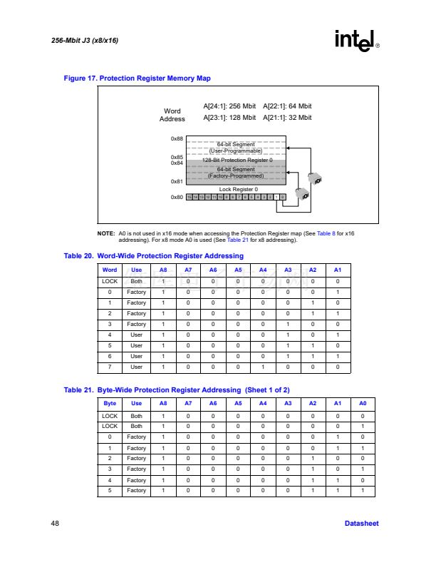
memory (J3) includes a 128-bit Protection Register (PR) that can be used to
increase the security of a system design. For example, the number contained in the PR can be used
to 鈥渕ate鈥?the flash component with other system components such as the CPU or ASIC, preventing
device substitution.
The 128-bits of the PR are divided into two 64-bit segments. One of the segments is programmed at
the Intel factory with a unique 64-bit number, which is unalterable. The other segment is left blank
for customer designers to program as desired. Once the customer segment is programmed, it can be
locked to prevent further programming.
13.3.1
Reading the Protection Register
The Protection Register is read in the identification read mode. The device is switched to this mode
by issuing the Read Identifier command (0x90). Once in this mode, read cycles from addresses
shown in
Table 8
or
Table 21
retrieve the specified information. To return to read array mode, write
the Read Array command (0xFF).
13.3.2
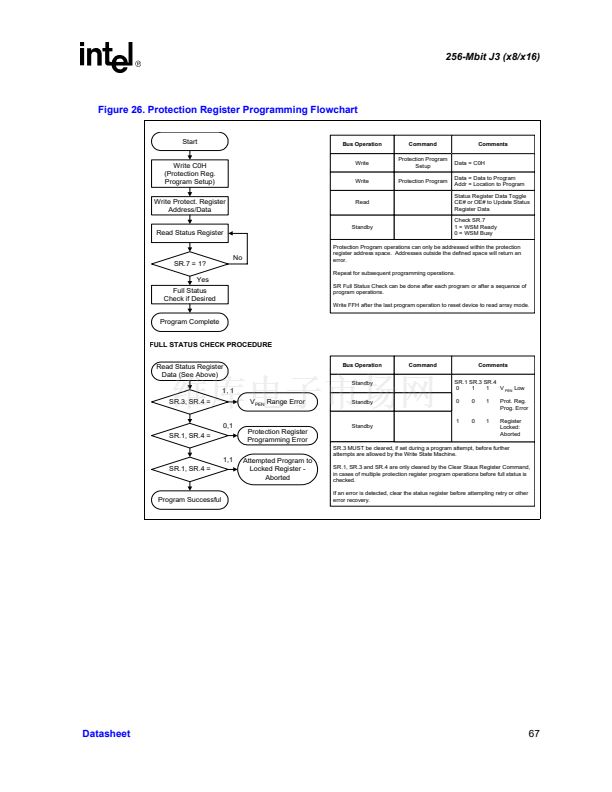
Programming the Protection Register
Protection Register bits are programmed using the two-cycle Protection Program command. The
64-bit number is programmed 16 bits at a time for word-wide configuration and eight bits at a time
for byte-wide configuration. First write the Protection Program Setup command, 0xC0. The next
write to the device will latch in address and data and program the specified location. The allowable
addresses are shown in
Table 8
or
Table 21.
See
Figure 26, 鈥淧rotection Register Programming
Flowchart鈥?on page 67
Any attempt to address Protection Program commands outside the defined PR address space will
result in a Status Register error (SR.4 will be set). Attempting to program a locked PR segment will
result in a Status Register error (SR.4 and SR.1 will be set).
13.3.3
Locking the Protection Register
The user-programmable segment of the Protection Register is lockable by programming Bit 1 of
the PLR to 0. Bit 0 of this location is programmed to 0 at the Intel factory to protect the unique
device number. Bit 1 is set using the Protection Program command to program 鈥?xFFFD鈥?to the
PLR. After these bits have been programmed, no further changes can be made to the values stored
in the Protection Register. Protection Program commands to a locked section will result in a Status
Register error (SR.4 and SR.1 will be set). PR lockout state is not reversible.
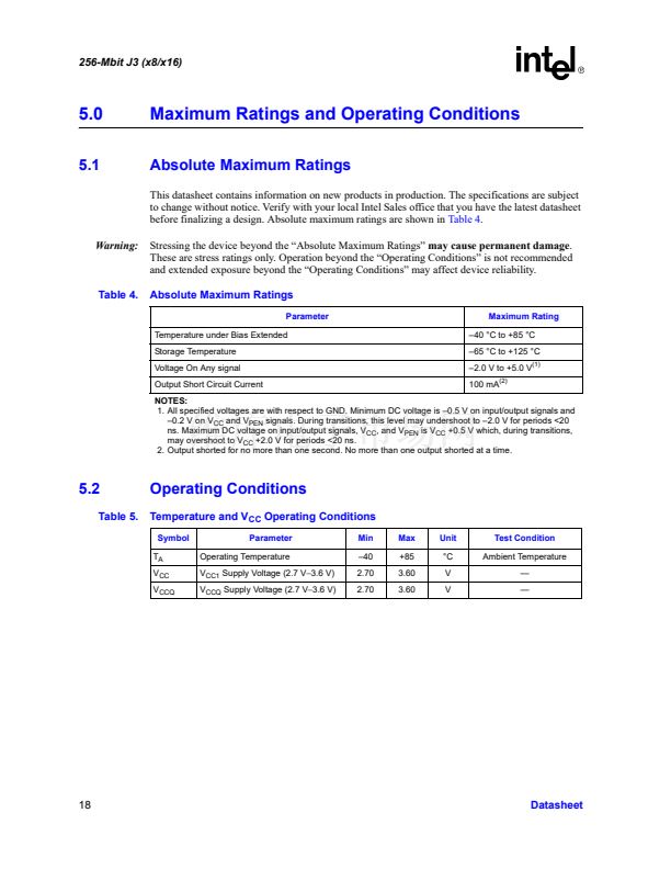
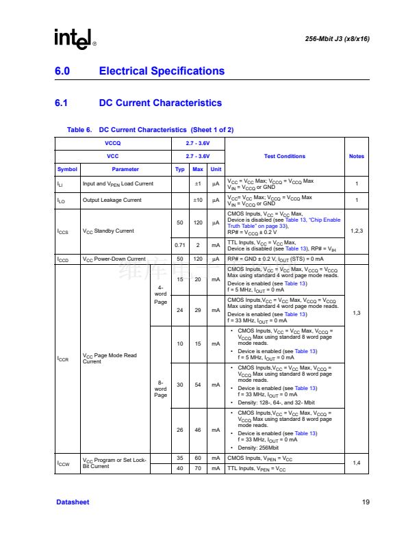
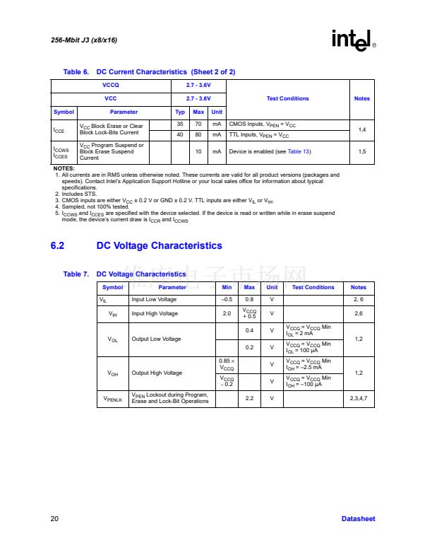
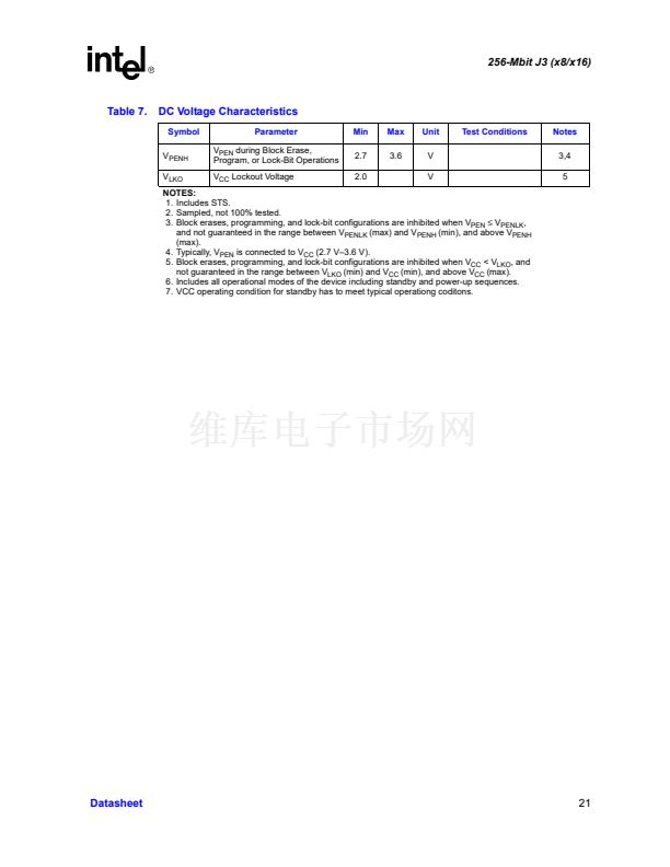
Datasheet
47


 1
1
 2
2
 3
3
 4
4
 5
5
 6
6
 7
7
 8
8
 9
9
 10
10
 11
11
 12
12
 13
13
 14
14
 15
15
 16
16
 17
17
 18
18
 19
19
 20
20
 21
21
 22
22
 23
23
 24
24
 25
25
 26
26
 27
27
 28
28
 29
29
 30
30
 31
31
 32
32
 33
33
 34
34
 35
35
 36
36
 37
37
 38
38
 39
39
 40
40
 41
41
 42
42
 43
43
 44
44
 45
45
 46
46
 47
47
 48
48
 49
49
 50
50
 51
51
 52
52
 53
53
 54
54
 55
55
 56
56
 57
57
 58
58
 59
59
 60
60
 61
61
 62
62
 63
63
 64
64
 65
65
 66
66
 67
67
 68
68
 69
69
 70
70
 71
71
 72
72
