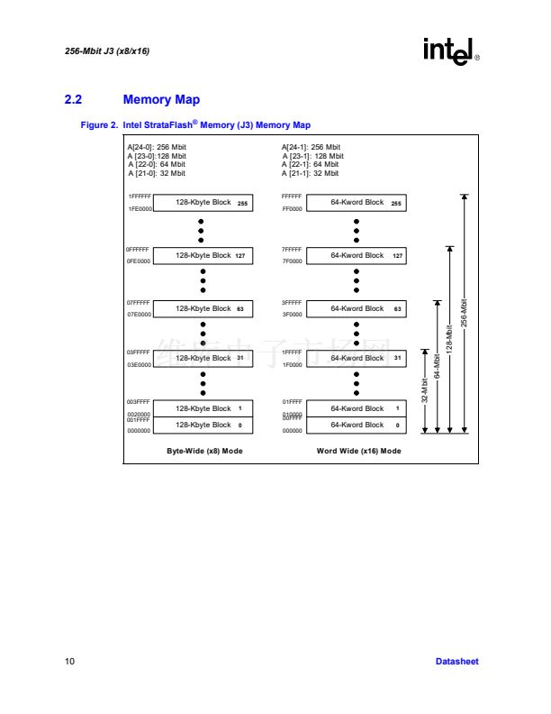
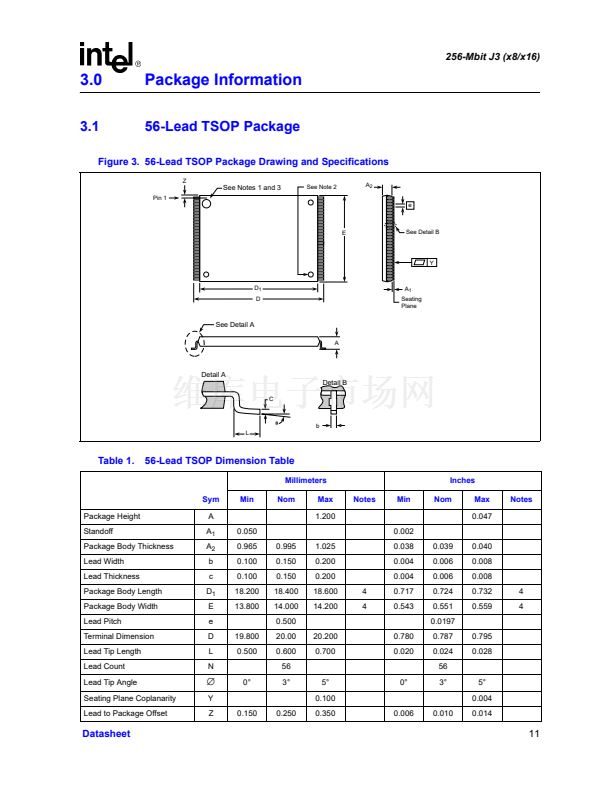
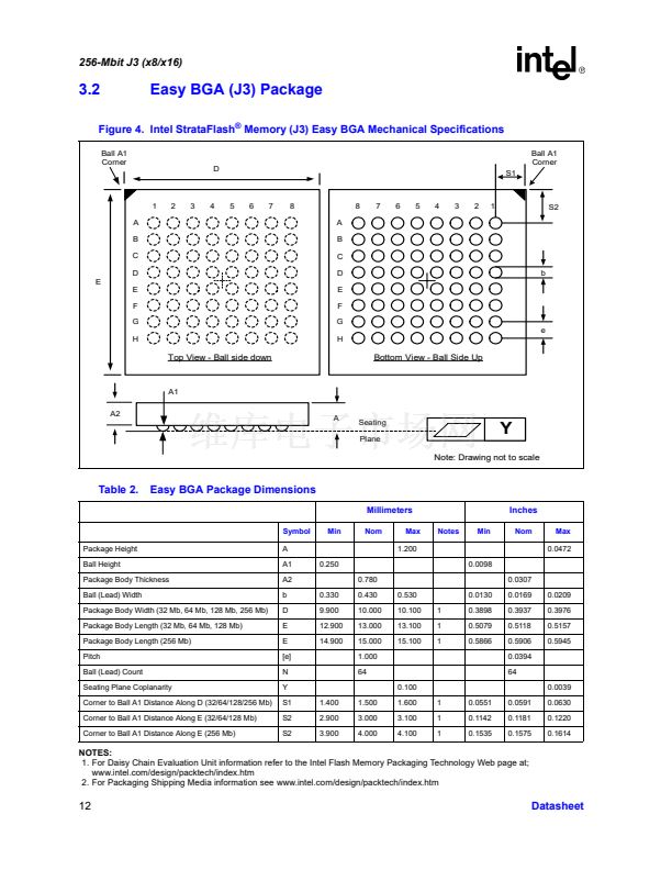
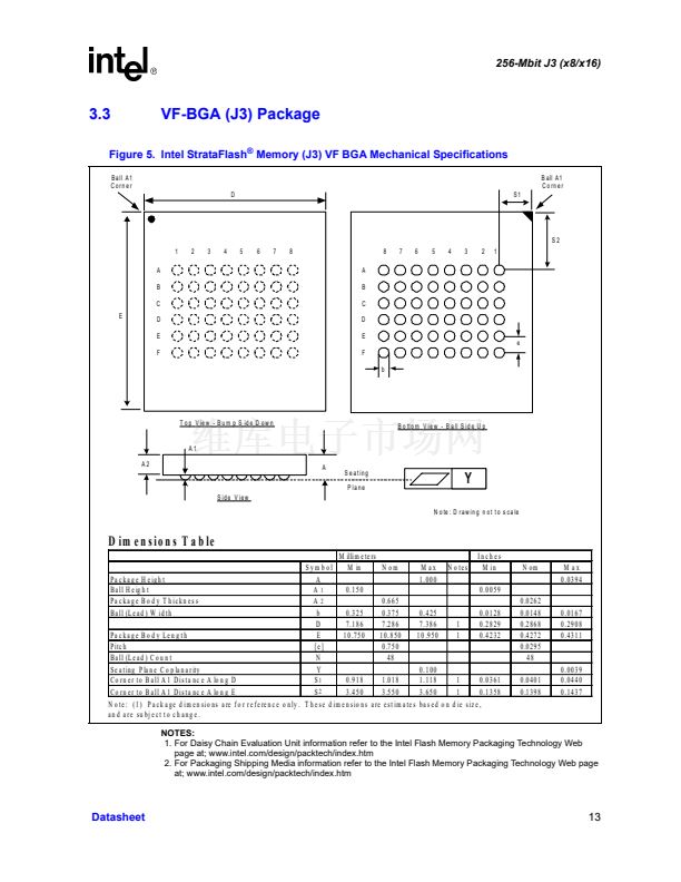
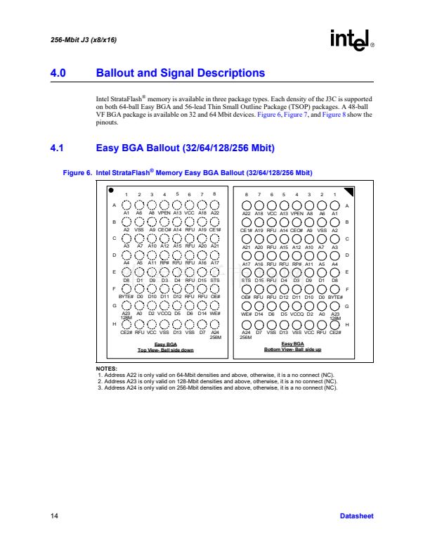
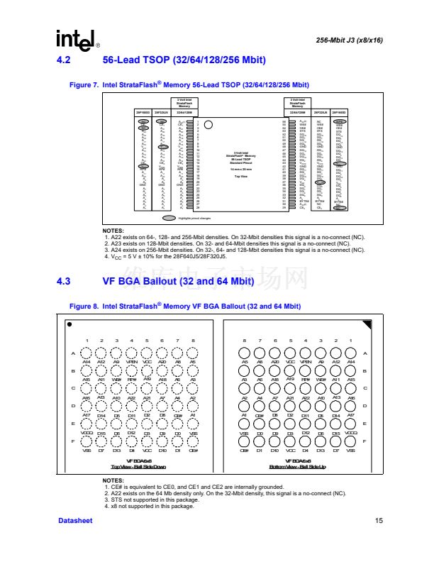
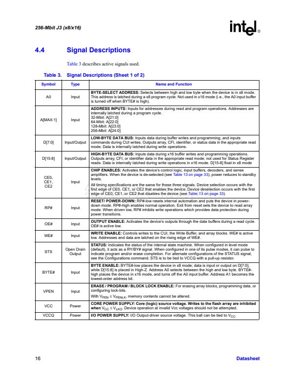
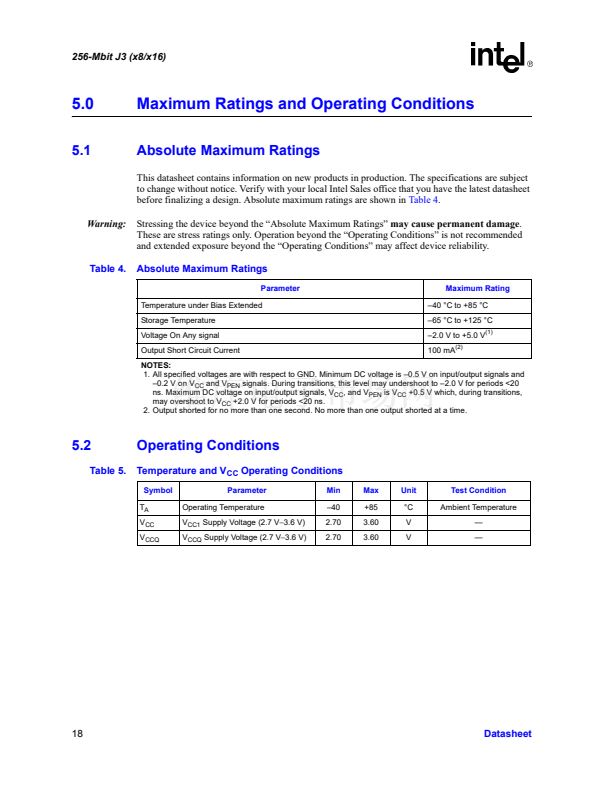
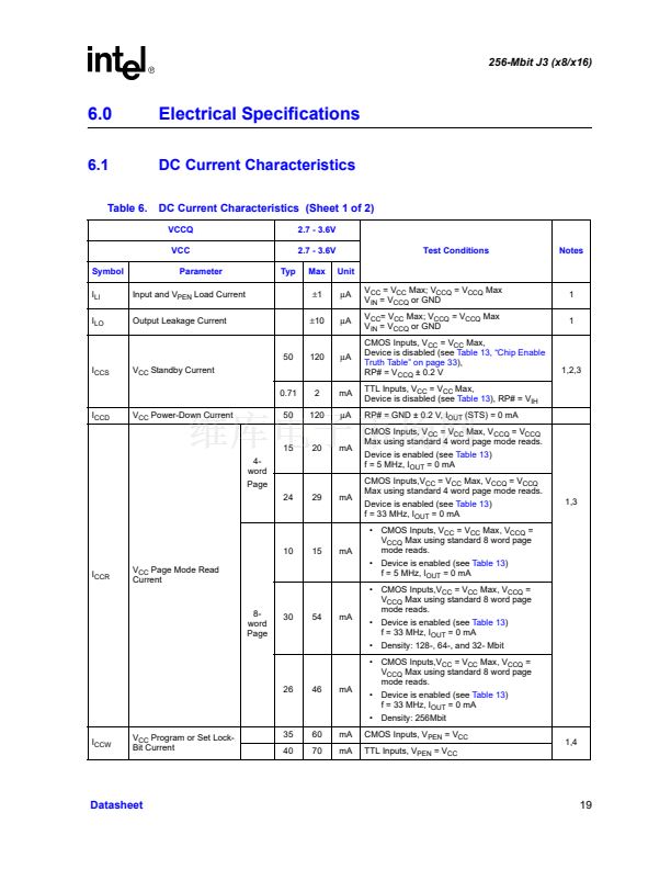
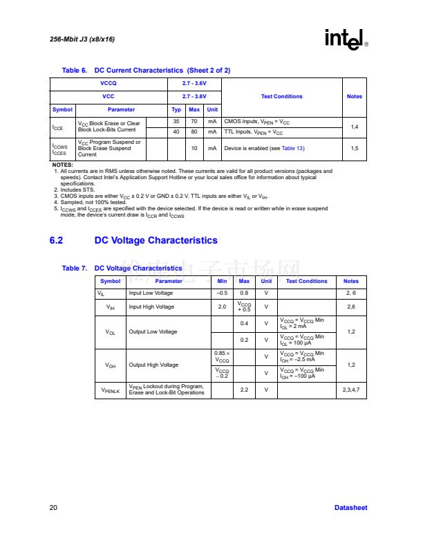
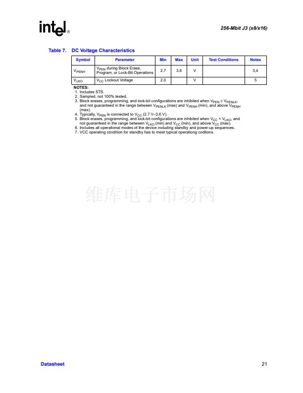
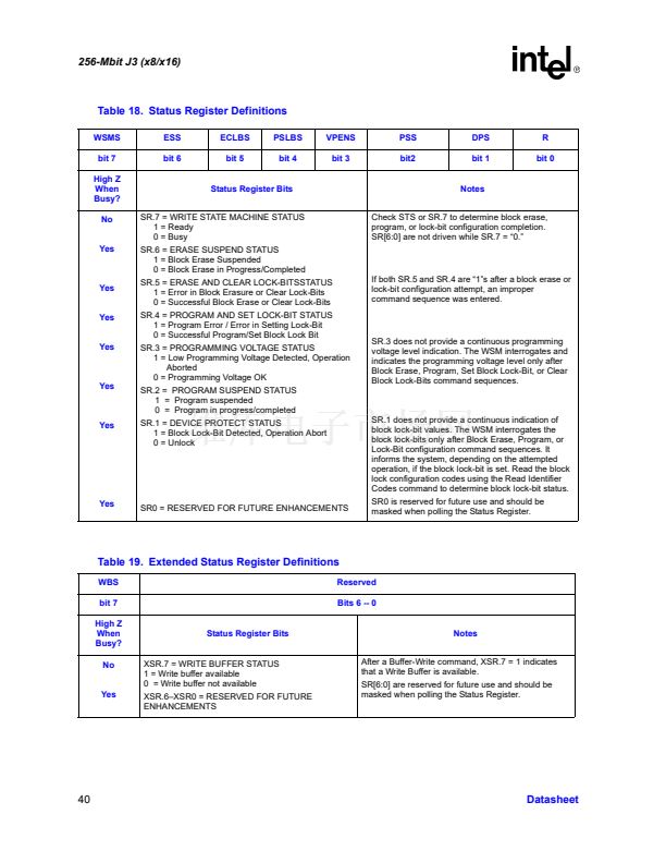
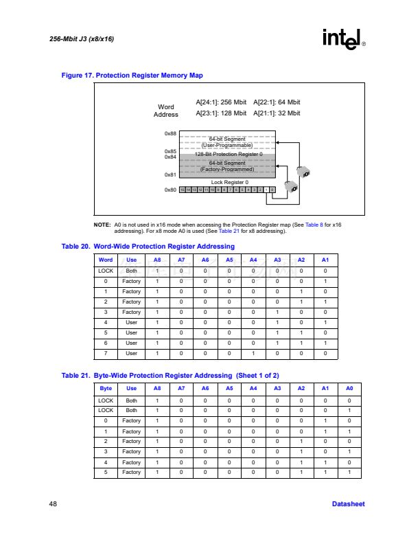
256-Mbit J3 (x8/x16)
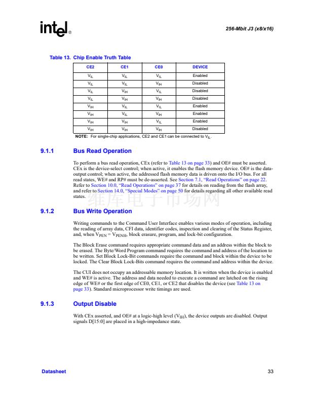
Table 21. Byte-Wide Protection Register Addressing (Sheet 2 of 2)
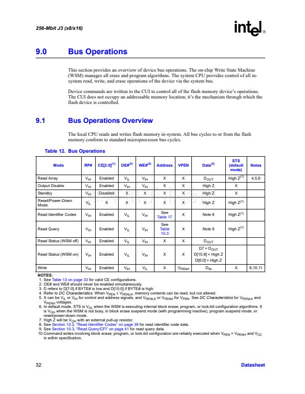
6
7
8
9
A
B
C
D
E
F
Factory
Factory
User
User
User
User
User
User
User
User
1
1
1
1
1
1
1
1
1
1
0
0
0
0
0
0
0
0
0
0
0
0
0
0
0
0
0
0
0
0
0
0
0
0
0
0
0
0
0
0
0
0
0
0
0
0
0
0
1
1
1
1
1
1
1
1
1
1
0
0
0
0
0
0
1
1
1
1
0
0
0
0
1
1
0
0
1
1
0
0
0
1
0
1
0
1
0
1
0
1
NOTE:
All address lines not specified in the above table must be 0 when accessing the Protection Register,
i.e.g., A[MAX:9] = 0.
13.4
Array Protection
The V
PEN
signal is a hardware mechanism to prohibit array alteration. When the V
PEN
voltage is
below the V
PENLK
voltage, array contents cannot be altered. To ensure a proper erase or program
operation, V
PEN
must be set to a valid voltage level. To determine the status of an erase or program
operation, poll the Status Register and analyze the bits.
Datasheet
49


 1
1
 2
2
 3
3
 4
4
 5
5
 6
6
 7
7
 8
8
 9
9
 10
10
 11
11
 12
12
 13
13
 14
14
 15
15
 16
16
 17
17
 18
18
 19
19
 20
20
 21
21
 22
22
 23
23
 24
24
 25
25
 26
26
 27
27
 28
28
 29
29
 30
30
 31
31
 32
32
 33
33
 34
34
 35
35
 36
36
 37
37
 38
38
 39
39
 40
40
 41
41
 42
42
 43
43
 44
44
 45
45
 46
46
 47
47
 48
48
 49
49
 50
50
 51
51
 52
52
 53
53
 54
54
 55
55
 56
56
 57
57
 58
58
 59
59
 60
60
 61
61
 62
62
 63
63
 64
64
 65
65
 66
66
 67
67
 68
68
 69
69
 70
70
 71
71
 72
72
