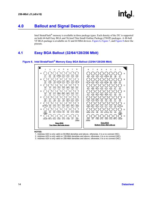
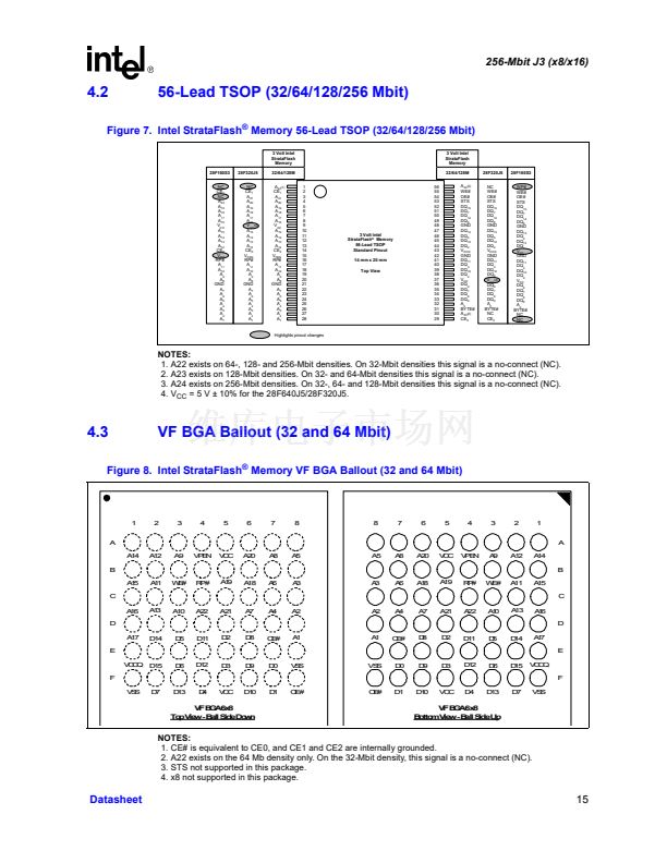
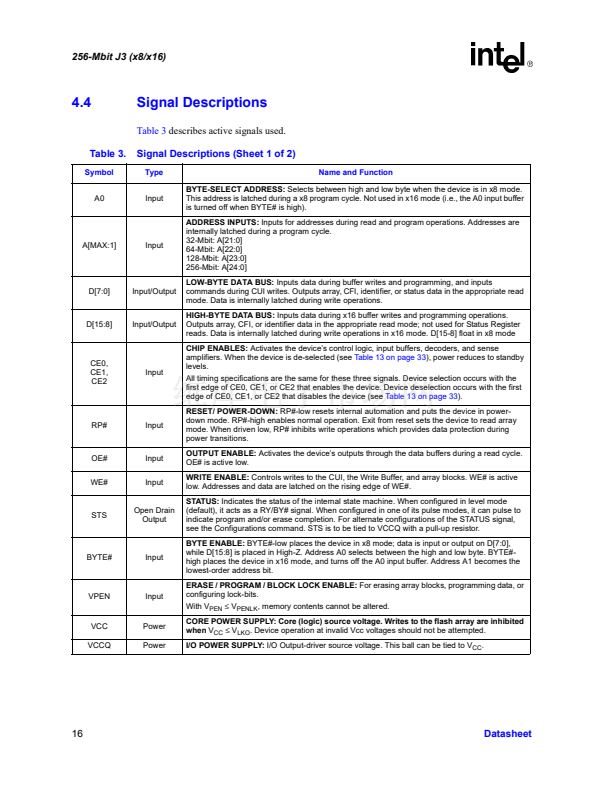
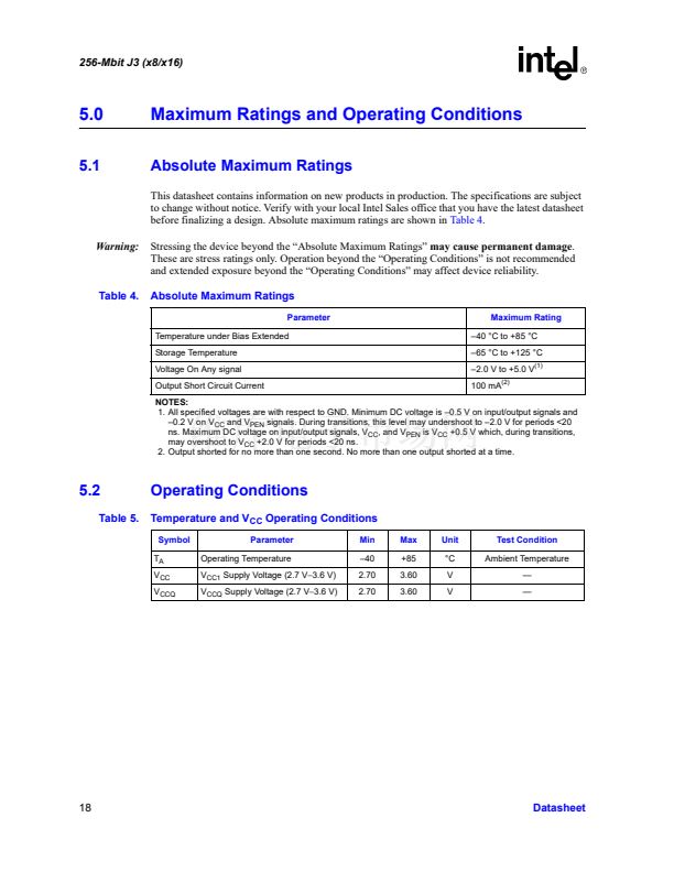
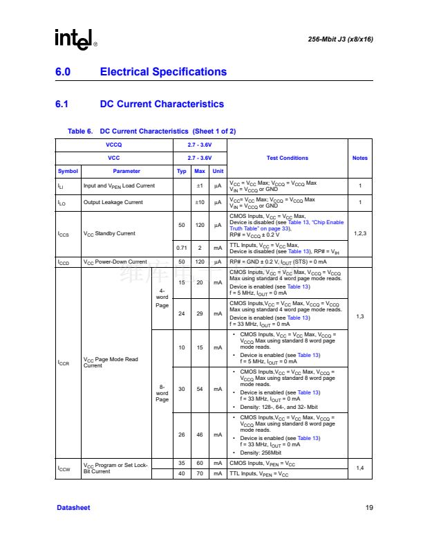
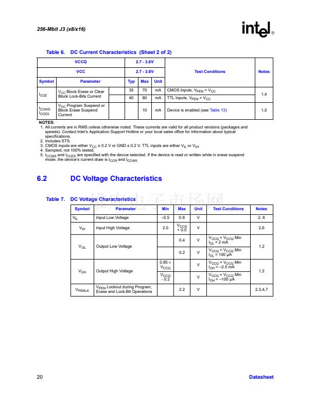
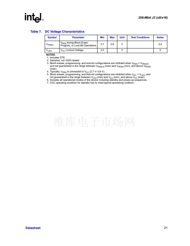
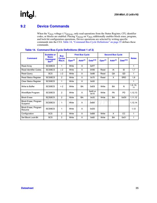
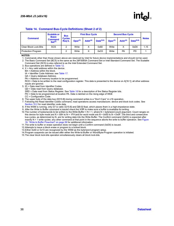
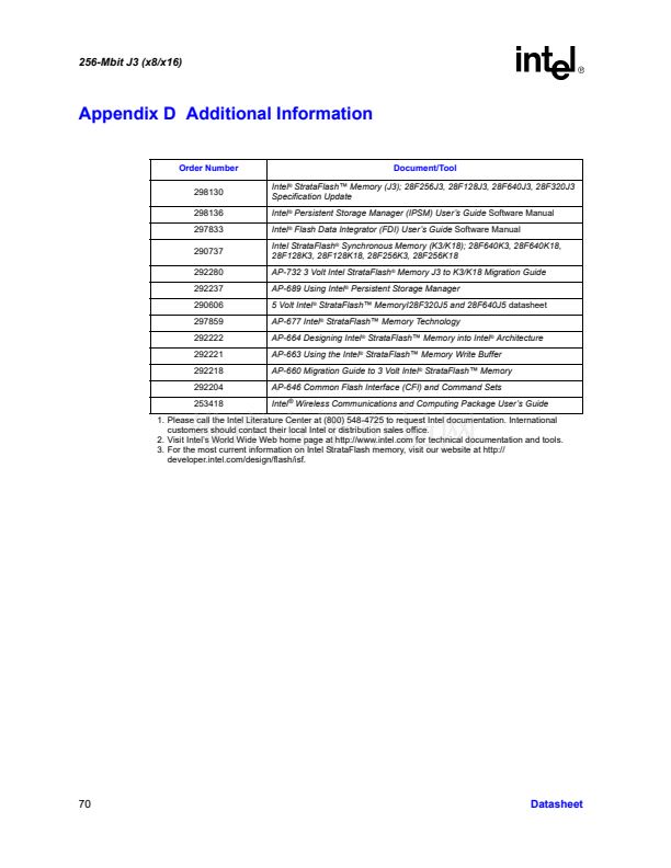
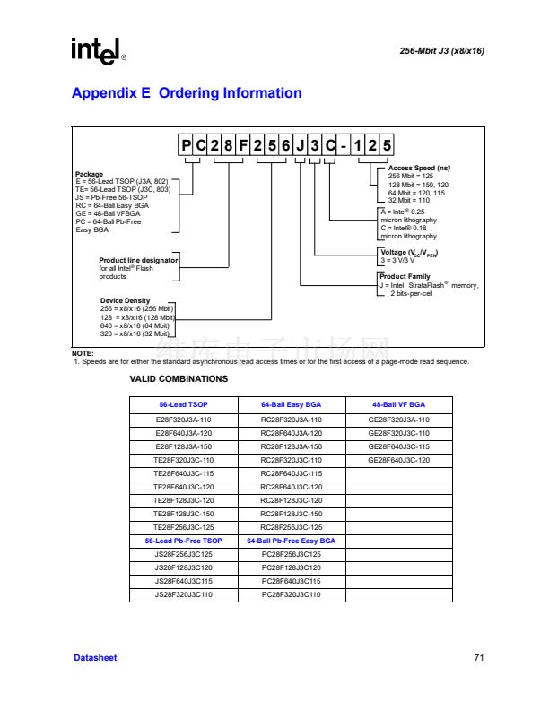
256-Mbit J3 (x8/x16)
Table 27. CFI Identification (Sheet 2 of 2)
Offset
Length
Description
0000h means no second vendor-specified algorithm exists
Secondary algorithm Extended Query Table address.
0000h means none exists
Add.
18:
19:
1A:
Hex
Code
--00
--00
--00
Value
19h
2
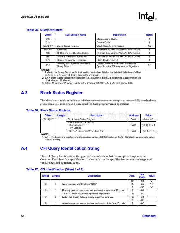
A.5
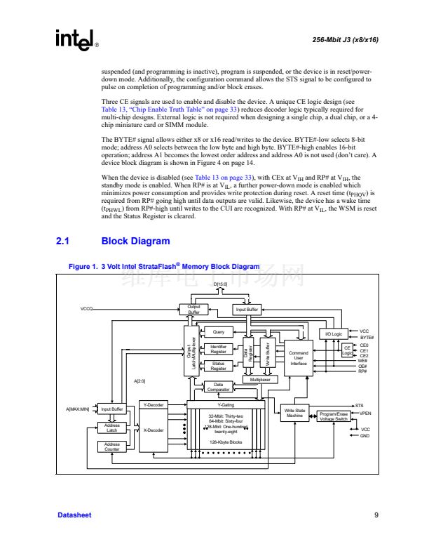
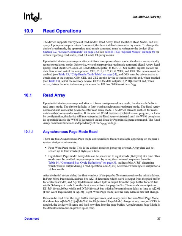
System Interface Information
The following device information can optimize system interface software.
Table 28. System Interface Information
Offset
1Bh
Length
1
Description
V
CC
logic supply minimum program/erase voltage
bits 0鈥? BCD 100 mV
bits 4鈥? BCD volts
V
CC
logic supply maximum program/erase voltage
bits 0鈥? BCD 100 mV
bits 4鈥? BCD volts
V
PP
[programming] supply minimum program/erase voltage
bits 0鈥? BCD 100 mV
bits 4鈥? HEX volts
V
PP
[programming] supply maximum program/erase voltage
bits 0鈥? BCD 100 mV
bits 4鈥? HEX volts
鈥渘鈥?such that typical single word program time-out = 2
n
碌s
鈥渘鈥?such that typical max. buffer write time-out = 2
n
碌s
鈥渘鈥?such that typical block erase time-out = 2
n
ms
鈥渘鈥?such that typical full chip erase time-out = 2
n
ms
鈥渘鈥?such that maximum word program time-out = 2
n
times
typical
鈥渘鈥?such that maximum buffer write time-out = 2
n
times typical
鈥渘鈥?such that maximum block erase time-out = 2
n
times typical
鈥渘鈥?such that maximum chip erase time-out = 2
n
times typical
Add.
1B:
Hex
Code
--27
Value
2.7 V
1Ch
1
1C:
--36
3.6 V
1Dh
1
1D:
--00
0.0 V
1Eh
1Fh
20h
21h
22h
23h
24h
25h
26h
1
1
1
1
1
1
1
1
1
1E:
1F:
20:
21:
22:
23:
24:
25:
26:
--00
--08
--08
--0A
--00
--04
--04
--04
--00
0.0 V
256 碌s
256 碌s
1s
NA
2 ms
2 ms
16 s
NA
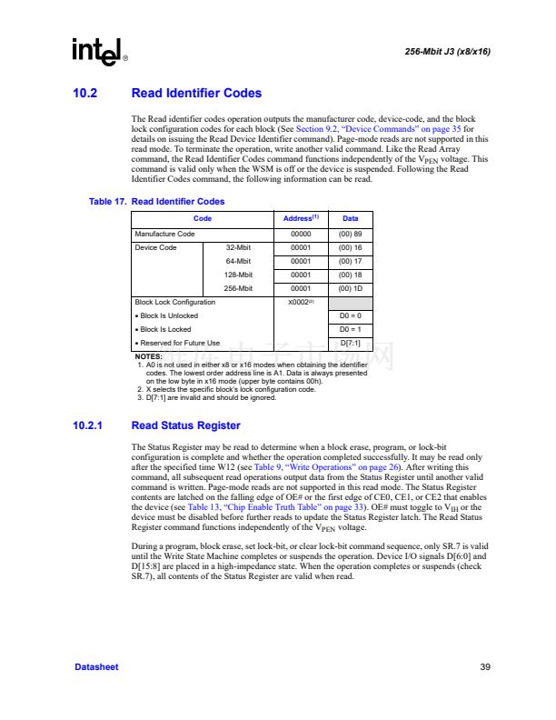
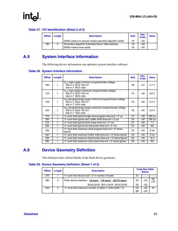
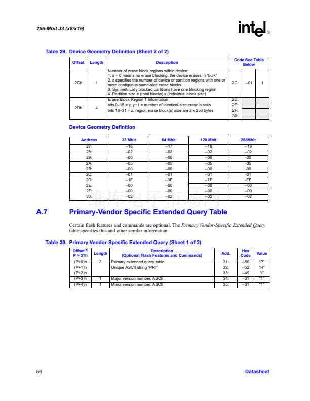
A.6
Device Geometry Definition
This field provides critical details of the flash device geometry.
Table 29. Device Geometry Definition (Sheet 1 of 2)
Offset
27h
28h
2Ah
Length
1
2
2
Description
鈥渘鈥?such that device size = 2
n
in number of bytes
Flash device interface: x8 async x16 async x8/x16 async
28:00,29:00 28:01,29:00 28:02,29:00
鈥渘鈥?such that maximum number of bytes in write buffer = 2
n
Code See Table
Below
27:
28:
29:
2A:
2B:
--02
--00
--05
--00
x8/
x16
32
Datasheet
55


 1
1
 2
2
 3
3
 4
4
 5
5
 6
6
 7
7
 8
8
 9
9
 10
10
 11
11
 12
12
 13
13
 14
14
 15
15
 16
16
 17
17
 18
18
 19
19
 20
20
 21
21
 22
22
 23
23
 24
24
 25
25
 26
26
 27
27
 28
28
 29
29
 30
30
 31
31
 32
32
 33
33
 34
34
 35
35
 36
36
 37
37
 38
38
 39
39
 40
40
 41
41
 42
42
 43
43
 44
44
 45
45
 46
46
 47
47
 48
48
 49
49
 50
50
 51
51
 52
52
 53
53
 54
54
 55
55
 56
56
 57
57
 58
58
 59
59
 60
60
 61
61
 62
62
 63
63
 64
64
 65
65
 66
66
 67
67
 68
68
 69
69
 70
70
 71
71
 72
72
