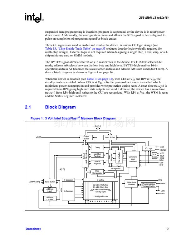
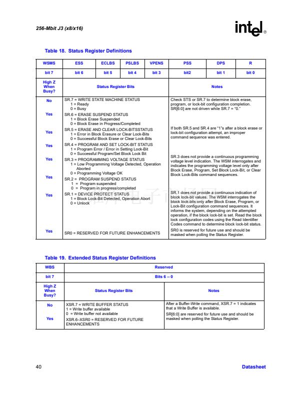
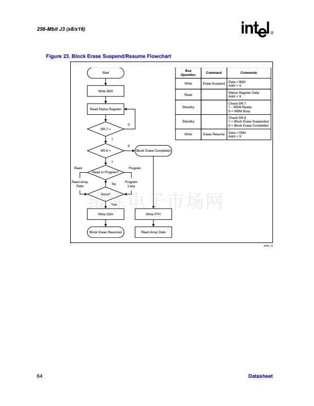
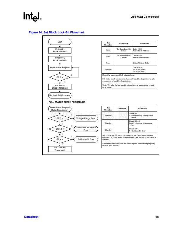
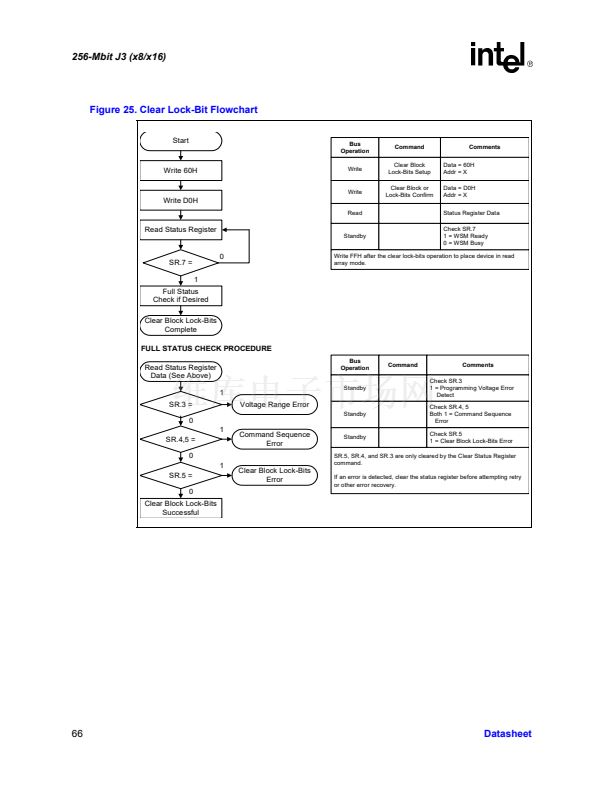
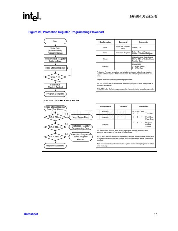
256-Mbit J3 (x8/x16)
Appendix C Design Considerations
C.1
Three-Line Output Control
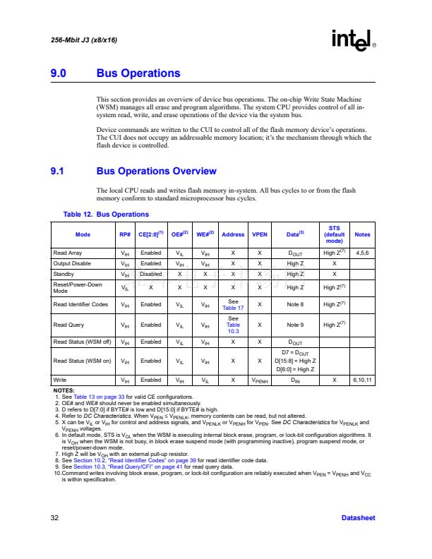
The device will often be used in large memory arrays. Intel provides five control inputs (CE0, CE1,
CE2, OE#, and RP#) to accommodate multiple memory connections. This control provides for:
a.
Lowest possible memory power dissipation.
b.
Complete assurance that data bus contention will not occur.
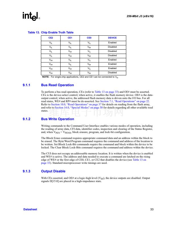
To use these control inputs efficiently, an address decoder should enable the device (see
Table 13)
while OE# should be connected to all memory devices and the system鈥檚 READ# control line. This
assures that only selected memory devices have active outputs while de-selected memory devices
are in standby mode. RP# should be connected to the system POWERGOOD signal to prevent
unintended writes during system power transitions. POWERGOOD should also toggle during
system reset.
C.2
STS and Block Erase, Program, and Lock-Bit Configuration
Polling
STS is an open drain output that should be connected to VCCQ by a pull-up resistor to provide a
hardware method of detecting block erase, program, and lock-bit configuration completion. It is
recommended that a 2.5k resister be used between STS# and VCCQ. In default mode, it transitions
low after block erase, program, or lock-bit configuration commands and returns to High Z when
the WSM has finished executing the internal algorithm. For alternate configurations of the STS
signal, see the Configuration command.
STS can be connected to an interrupt input of the system CPU or controller. It is active at all times.
STS, in default mode, is also High Z when the device is in block erase suspend (with programming
inactive), program suspend, or in reset/power-down mode.
C.3
Input Signal Transitions鈥擱educing Overshoots and
Undershoots When Using Buffers or Transceivers
As faster, high-drive devices such as transceivers or buffers drive input signals to flash memory
devices, overshoots and undershoots can sometimes cause input signals to exceed flash memory
specifications. (See 鈥淒C Voltage Characteristics鈥?on page 20.) Many buffer/transceiver vendors
now carry bus-interface devices with internal output-damping resistors or reduced-drive outputs.
Internal output-damping resistors diminish the nominal output drive currents, while still leaving
sufficient drive capability for most applications. These internal output-damping resistors help
reduce unnecessary overshoots and undershoots. Transceivers or buffers with balanced- or light-
drive outputs also reduce overshoots and undershoots by diminishing output-drive currents. When
considering a buffer/transceiver interface design to flash, devices with internal output-damping
resistors or reduced-drive outputs should be used to minimize overshoots and undershoots. For
additional information, please refer to AP-647,
5 Volt Intel StrataFlash
庐
Memory Design Guide
(Order Number: 292205).
68
Datasheet


 1
1
 2
2
 3
3
 4
4
 5
5
 6
6
 7
7
 8
8
 9
9
 10
10
 11
11
 12
12
 13
13
 14
14
 15
15
 16
16
 17
17
 18
18
 19
19
 20
20
 21
21
 22
22
 23
23
 24
24
 25
25
 26
26
 27
27
 28
28
 29
29
 30
30
 31
31
 32
32
 33
33
 34
34
 35
35
 36
36
 37
37
 38
38
 39
39
 40
40
 41
41
 42
42
 43
43
 44
44
 45
45
 46
46
 47
47
 48
48
 49
49
 50
50
 51
51
 52
52
 53
53
 54
54
 55
55
 56
56
 57
57
 58
58
 59
59
 60
60
 61
61
 62
62
 63
63
 64
64
 65
65
 66
66
 67
67
 68
68
 69
69
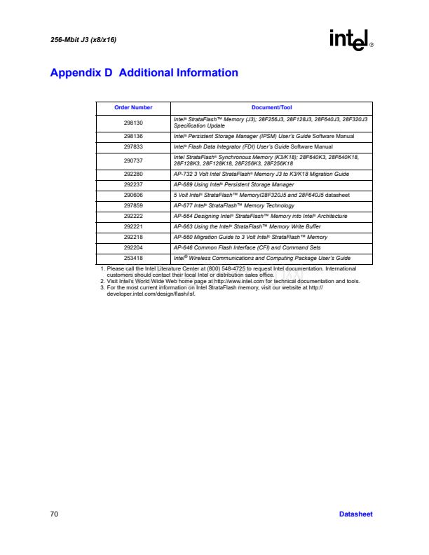 70
70
 71
71
 72
72
