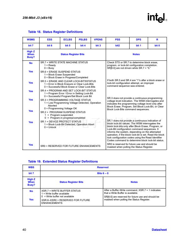
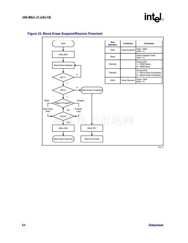
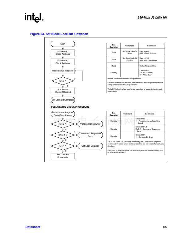
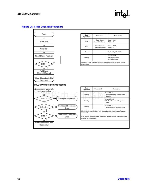
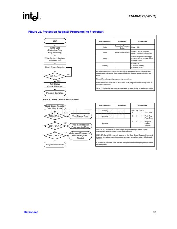
256-Mbit J3 (x8/x16)
1.0
Introduction
This document describes the Intel StrataFlash
庐
Memory (J3) device. It includes a description of
device features, operations, and specifications.
1.1
Nomenclature
AMIN:
AMAX:
AMIN = A0 for x8
AMIN = A1 for x16
32 Mbit
AMAX = A21
64 Mbit
AMAX = A22
128 Mbit
AMAX = A23
256 Mbit
AMAX = A24
A group of flash cells that share common erase circuitry and erase simultaneously
Indicates a logic zero (0)
Command User Interface
Multi-Level Cell
One Time Programmable
Protection Lock Register
Protection Register
Protection Register Data
To write data to the flash array
Reserved for Future Use
Indicates a logic one (1)
Status Register
Status Register Data
Refers to a signal or package connection name
Refers to timing or voltage levels
Write State Machine
Extended Configuration Register
eXtended Status Register
Block:
Clear:
CUI:
MLC:
OTP:
PLR:
PR:
PRD
Program:
RFU:
Set:
SR:
SRD:
VPEN:
V
PEN
:
WSM:
ECR:
XSR:
1.2
Conventions
0x:
0b:
k (noun):
M (noun):
Nibble
Byte:
Word:
Kword:
Kb:
KB:
Mb:
MB:
Brackets:
Hexadecimal prefix
Binary prefix
1,000
1,000,000
4 bits
8 bits
16 bits
1,024 words
1,024 bits
1,024 bytes
1,048,576 bits
1,048,576 bytes
Square brackets ([]) will be used to designate group membership or to define a
group of signals with similar function (i.e., A[21:1], SR[4,1] and D[15:0]).
Datasheet
7


 1
1
 2
2
 3
3
 4
4
 5
5
 6
6
 7
7
 8
8
 9
9
 10
10
 11
11
 12
12
 13
13
 14
14
 15
15
 16
16
 17
17
 18
18
 19
19
 20
20
 21
21
 22
22
 23
23
 24
24
 25
25
 26
26
 27
27
 28
28
 29
29
 30
30
 31
31
 32
32
 33
33
 34
34
 35
35
 36
36
 37
37
 38
38
 39
39
 40
40
 41
41
 42
42
 43
43
 44
44
 45
45
 46
46
 47
47
 48
48
 49
49
 50
50
 51
51
 52
52
 53
53
 54
54
 55
55
 56
56
 57
57
 58
58
 59
59
 60
60
 61
61
 62
62
 63
63
 64
64
 65
65
 66
66
 67
67
 68
68
 69
69
 70
70
 71
71
 72
72
