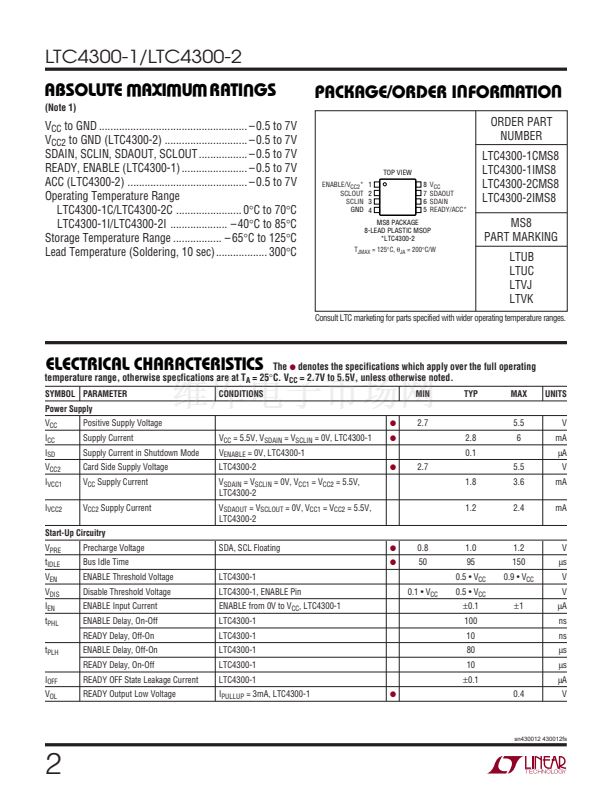
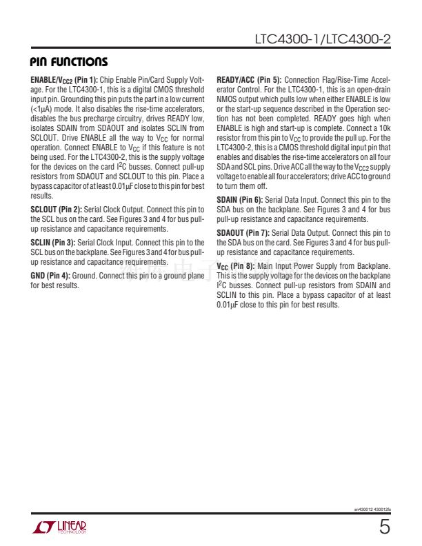
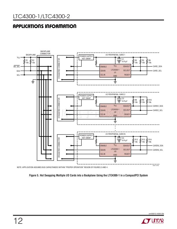
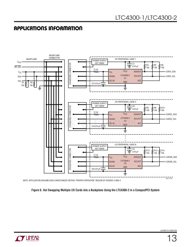
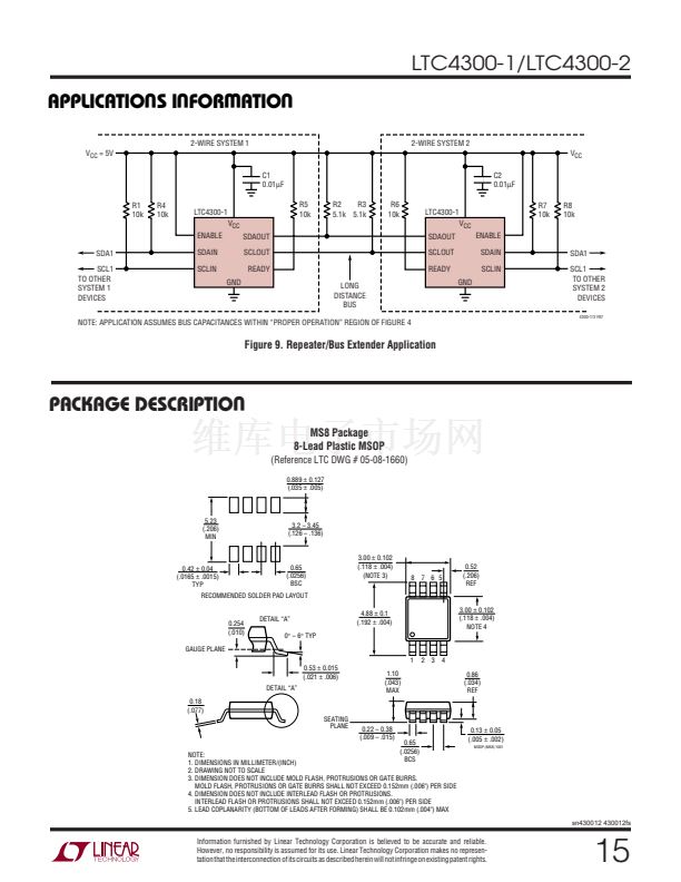
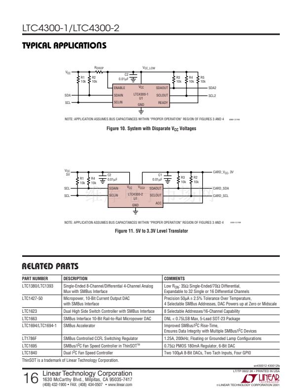
LTC4300-1/LTC4300-2
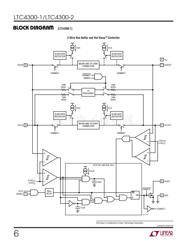
OPERATIO
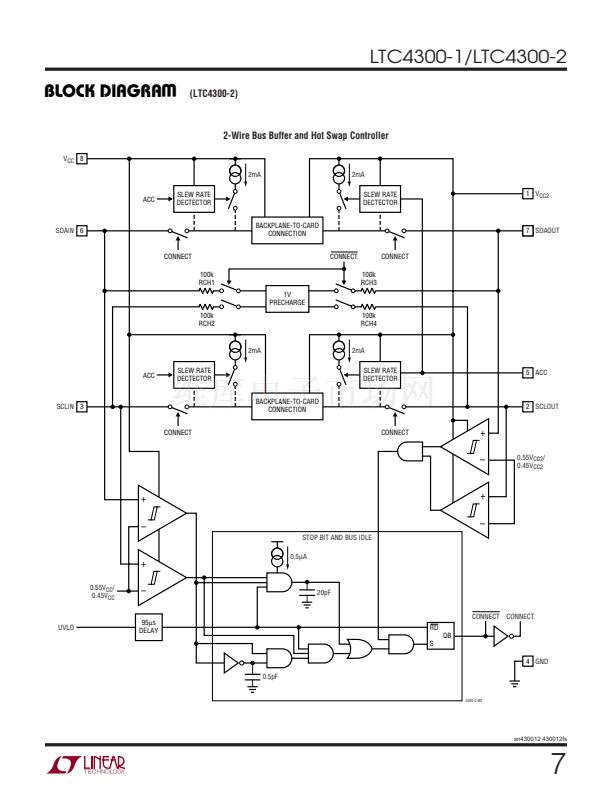
Start-Up
When the LTC4300 first receives power on its V
CC
pin,
either during power-up or during hot swapping, it starts in
an undervoltage lockout (UVLO) state, ignoring any activ-
ity on the SDA and SCL pins until V
CC
rises above 2.5V. For
the LTC4300-2, the part also waits for V
CC2
to rise above
2V. This ensures that the part does not try to function until
it has enough voltage to do so.
During this time, the 1V precharge circuitry is also active
and forces 1V through 100k nominal resistors to the SDA
and SCL pins. Because the I/O card is being plugged into
a live backplane, the voltage on the backplane SDA and SCL
busses may be anywhere between 0V and V
CC
. Precharging
the SCL and SDA pins to 1V minimizes the worst-case
voltage differential these pins will see at the moment of con-
nection, therefore minimizing the amount of disturbance
caused by the I/O card.
Once the LTC4300 comes out of UVLO, it assumes that
SDAIN and SCLIN have been hot swapped into a live
system and that SDAOUT and SCLOUT are being powered
up at the same time as itself. Therefore, it looks for either
a stop bit or bus idle condition on the backplane side to
indicate the completion of a data transaction. When either
one occurs, the part also verifies that both the SDAOUT
and SCLOUT voltages are high. When all of these condi-
tions are met, the input-to-output connection circuitry is
activated, joining the SDA and SCL busses on the I/O card
with those on the backplane.
Connection Circuitry
Once the connection circuitry is activated, the functional-
ity of the SDAIN and SDAOUT pins is identical. A low forced
on either pin at any time results in both pin voltages being
low. SDAIN and SDAOUT enter a logic high state only when
all devices on both SDAIN and SDAOUT force a high. The
same is true for SCLIN and SCLOUT. This important fea-
ture ensures that clock stretching, clock arbitration and the
acknowledge protocol always work, regardless of how the
devices in the system are tied to the LTC4300.
Another key feature of the connection circuitry is that it
provides bidirectional buffering, keeping the backplane
and card capacitances isolated. Because of this isolation,
8
U
the waveforms on the backplane busses look slightly
different than the corresponding card bus waveforms, as
described here.
Input to Output Offset Voltage
When a logic low voltage, V
LOW1
, is driven on any of the
LTC4300鈥檚 data or clock pins, the LTC4300 regulates the
voltage on the other side of the chip (call it V
LOW2
) to a
slightly higher voltage, as directed by the following
equation:
V
LOW2
= V
LOW1
+ 50mV + (V
CC
/R) 鈥?100
where R is the bus pull-up resistance in ohms. For ex-
ample, if a device is forcing SDAOUT to 10mV and if
V
CC
= 3.3V and the pull-up resistor R on SDAIN is 10k, then
the voltage on SDAIN = 10mV + 50mV + (3.3/10000) 鈥?100
= 93mV. See the Typical Performance Characteristics
section for curves showing the offset voltage as a function
of V
CC
and R.
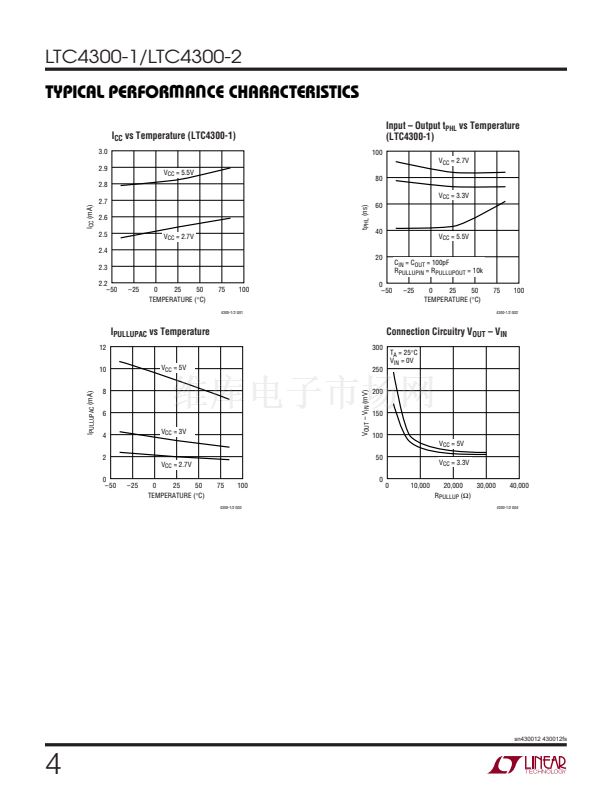
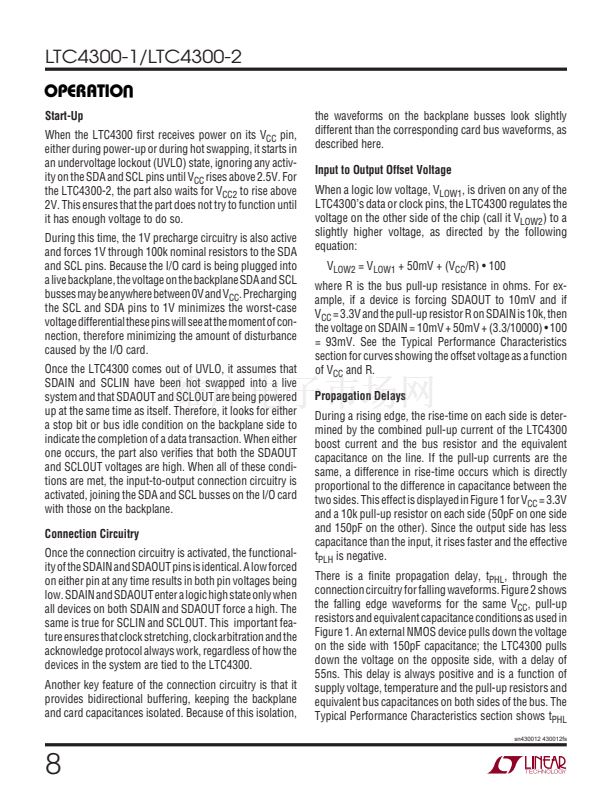
Propagation Delays
During a rising edge, the rise-time on each side is deter-
mined by the combined pull-up current of the LTC4300
boost current and the bus resistor and the equivalent
capacitance on the line. If the pull-up currents are the
same, a difference in rise-time occurs which is directly
proportional to the difference in capacitance between the
two sides. This effect is displayed in Figure 1 for V
CC
= 3.3V
and a 10k pull-up resistor on each side (50pF on one side
and 150pF on the other). Since the output side has less
capacitance than the input, it rises faster and the effective
t
PLH
is negative.
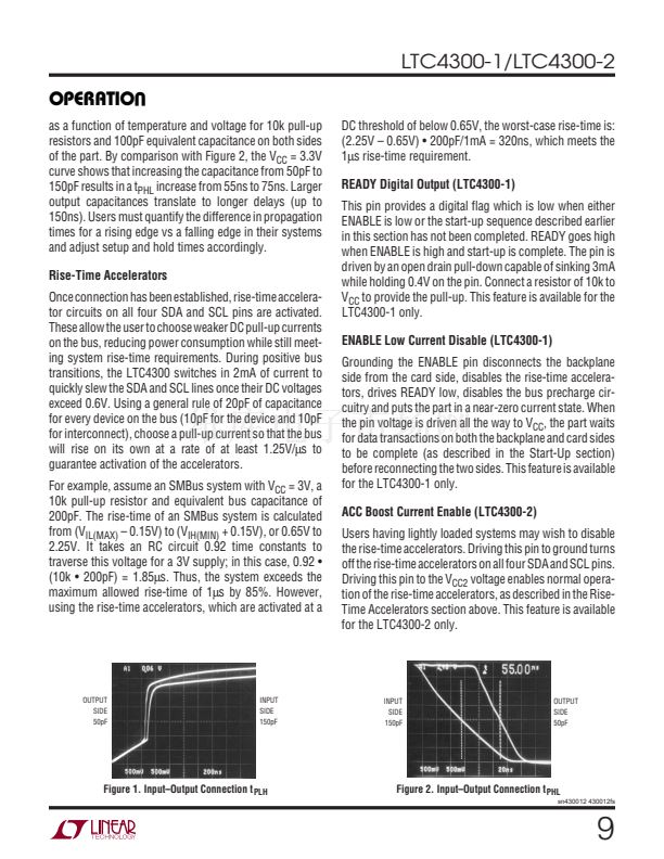
There is a finite propagation delay, t
PHL
, through the
connection circuitry for falling waveforms. Figure 2 shows
the falling edge waveforms for the same V
CC
, pull-up
resistors and equivalent capacitance conditions as used in
Figure 1. An external NMOS device pulls down the voltage
on the side with 150pF capacitance; the LTC4300 pulls
down the voltage on the opposite side, with a delay of
55ns. This delay is always positive and is a function of
supply voltage, temperature and the pull-up resistors and
equivalent bus capacitances on both sides of the bus. The
Typical Performance Characteristics section shows t
PHL
sn430012 430012fs


 1
1
 2
2
 3
3
 4
4
 5
5
 6
6
 7
7
 8
8
 9
9
 10
10
 11
11
 12
12
 13
13
 14
14
 15
15
 16
16
