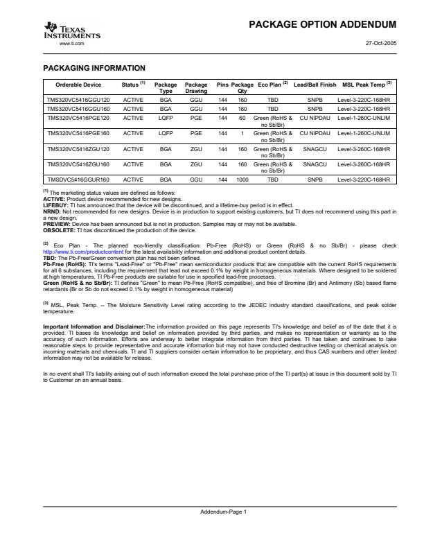
www.ti.com
TMS320VC5416
Fixed-Point Digital Signal Processor
SPRS095O 鈥?MARCH 1999 鈥?REVISED JANUARY 2005
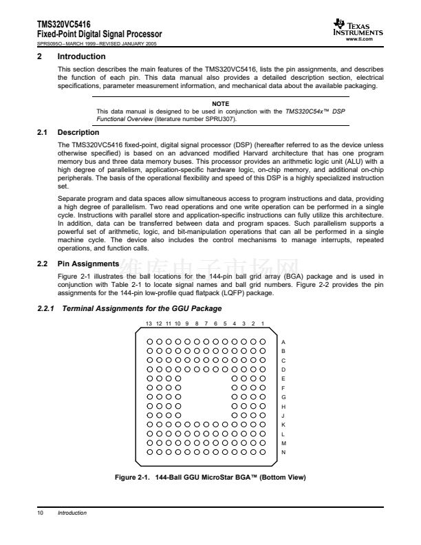
2.2.3
Signal Descriptions
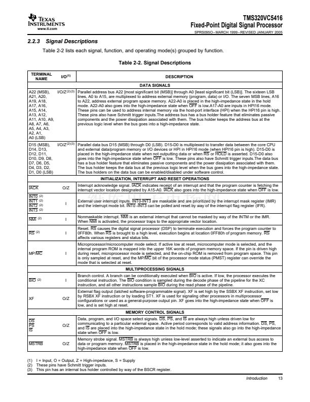
Table 2-2 lists each signal, function, and operating mode(s) grouped by function.
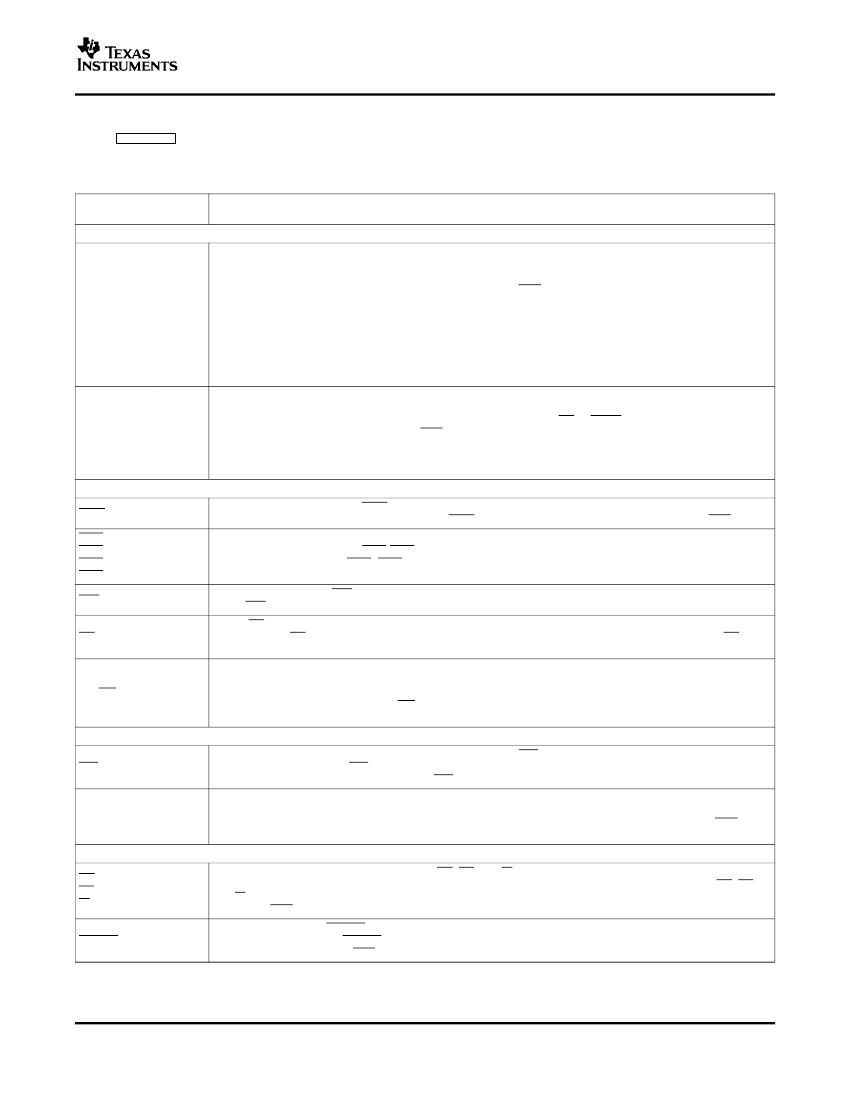
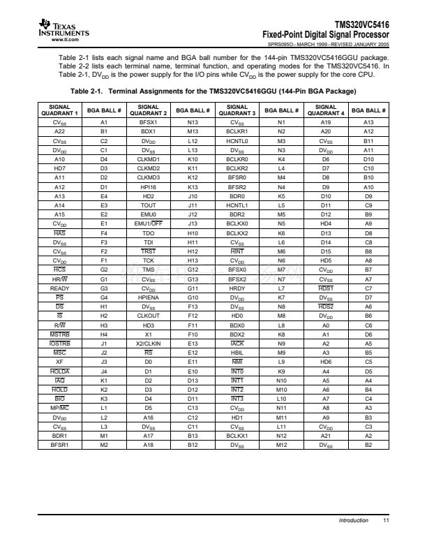
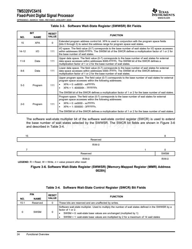
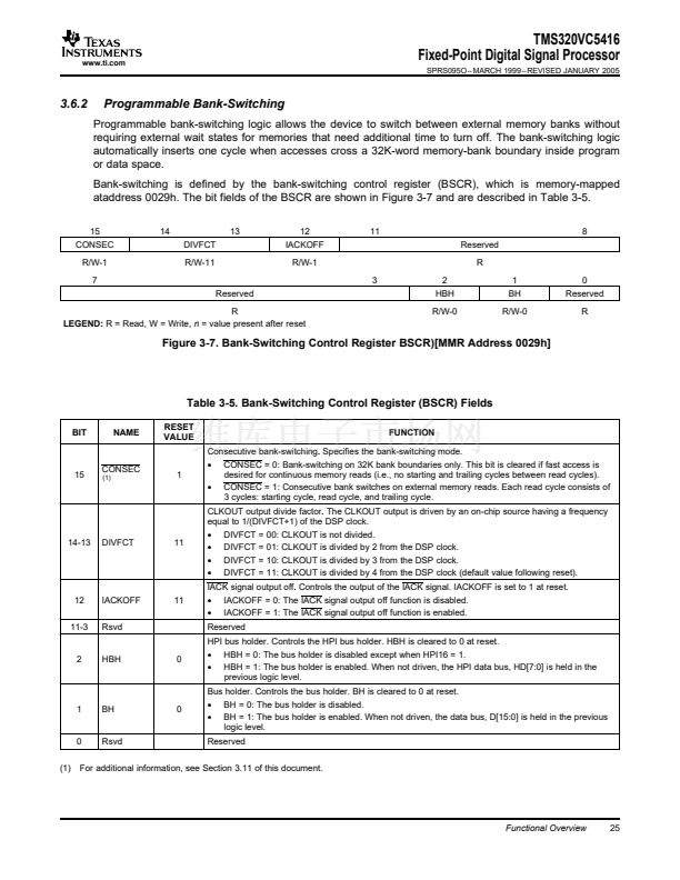
Table 2-2. Signal Descriptions
TERMINAL
NAME
I/O
(1)
DESCRIPTION
DATA SIGNALS
A22 (MSB),
I/O/Z
(2) (3)
A21, A20,
A19, A18,
A17, A16,
A15, A14,
A13, A12,
A11, A10, A9,
A8, A7, A6,
A5, A4, A3,
A2, A1,
A0 (LSB)
D15 (MSB),
D14, D13,
D12, D11,
D10, D9, D8,
D7, D6, D5,
D4, D3, D2,
D1, D0 (LSB)
Parallel address bus A22 [most significant bit (MSB)] through A0 [least significant bit (LSB)]. The sixteen LSB
lines, A0 to A15, are multiplexed to address external memory (program, data) or I/O. The seven MSB lines, A16
to A22, address external program space memory. A22-A0 is placed in the high-impedance state in the hold
mode. A22-A0 also goes into the high-impedance state when OFF is low.A17-A0 are inputs in HPI16 mode.
These pins can be used to address internal memory via the host-port interface (HPI) when the HPI16 pin is high.
These pins also have Schmitt trigger inputs.The address bus has a bus holder feature that eliminates passive
components and the power dissipation associated with them. The bus holder keeps the address bus at the
previous logic level when the bus goes into a high-impedance state.
I/O/Z
(2) (3)
Parallel data bus D15 (MSB) through D0 (LSB). D15-D0 is multiplexed to transfer data between the core CPU
and external data/program memory or I/O devices or HPI in HPI16 mode (when HPI16 pin is high). D15-D0 is
placed in the high-impedance state when not outputting data or when RS or HOLD is asserted. D15-D0 also
goes into the high-impedance state when OFF is low. These pins also have Schmitt trigger inputs.The data bus
has a bus holder feature that eliminates passive components and the power dissipation associated with them.
The bus holder keeps the data bus at the previous logic level when the bus goes into the high-impedance state.
The bus holders on the data bus can be enabled/disabled under software control.
INITIALIZATION, INTERRUPT AND RESET OPERATIONS
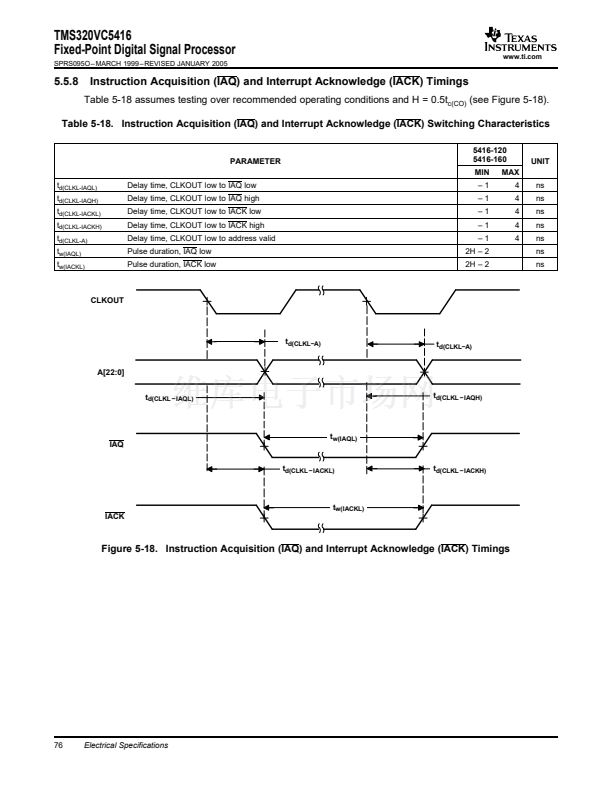
Interrupt acknowledge signal. IACK indicates receipt of an interrupt and that the program counter is fetching the
interrupt vector location designated by A15-A0. IACK also goes into the high-impedance state when OFF is low.
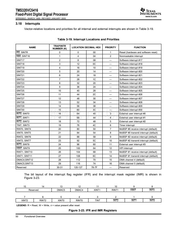
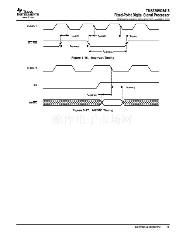
External user interrupt inputs. INT0-INT3 are maskable and are prioritized by the interrupt mask register (IMR)
and the interrupt mode bit. INT0 -INT3 can be polled and reset by way of the interrupt flag register (IFR).
Nonmaskable interrupt. NMI is an external interrupt that cannot be masked by way of the INTM or the IMR.
When NMI is activated, the processor traps to the appropriate vector location.
Reset. RS causes the digital signal processor (DSP) to terminate execution and forces the program counter to
0FF80h. When RS is brought to a high level, execution begins at location 0FF80h of program memory. RS
affects various registers and status bits.
Microprocessor/microcomputer mode select. If active low at reset, microcomputer mode is selected, and the
internal program ROM is mapped into the upper 16K words of program memory space. If the pin is driven high
during reset, microprocessor mode is selected, and the on-chip ROM is removed from program space. This pin
is only sampled at reset, and the MP/MC bit of the processor mode status (PMST) register can override the
mode that is selected at reset.
MULTIPROCESSING SIGNALS
Branch control. A branch can be conditionally executed when BIO is active. If low, the processor executes the
conditional instruction. The BIO condition is sampled during the decode phase of the pipeline for the XC
instruction, and all other instructions sample BIO during the read phase of the pipeline.
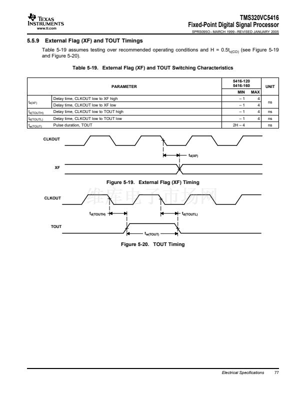
External flag output (latched software-programmable signal). XF is set high by the SSBX XF instruction, set low
by RSBX XF instruction or by loading ST1. XF is used for signaling other processors in multiprocessor
configurations or used as a general-purpose output pin. XF goes into the high-impedance state when OFF is
low, and is set high at reset.
MEMORY CONTROL SIGNALS
Data, program, and I/O space select signals. DS, PS, and IS are always high unless driven low for
communicating to a particular external space. Active period corresponds to valid address information. DS, PS,
and IS are placed into the high-impedance state in the hold mode; these signals also go into the high-impedance
state when OFF is low.
Memory strobe signal. MSTRB is always high unless low-level asserted to indicate an external bus access to
data or program memory. MSTRB is placed in the high-impedance state in the hold mode; it also goes into the
high-impedance state when OFF is low.
IACK
INT0
INT1
INT2
INT3
NMI
RS
(2)
(2)
(2)
(2)
(2)
O/Z
I
I
I
(2)
MP/MC
I
BIO
(2)
I
XF
O/Z
DS
PS
IS
MSTRB
O/Z
O/Z
(1)
(2)
(3)
I = Input, O = Output, Z = High-impedance, S = Supply
These pins have Schmitt trigger inputs.
This pin has an internal bus holder controlled by way of the BSCR register.
Introduction
13


 1
1
 2
2
 3
3
 4
4
 5
5
 6
6
 7
7
 8
8
 9
9
 10
10
 11
11
 12
12
 13
13
 14
14
 15
15
 16
16
 17
17
 18
18
 19
19
 20
20
 21
21
 22
22
 23
23
 24
24
 25
25
 26
26
 27
27
 28
28
 29
29
 30
30
 31
31
 32
32
 33
33
 34
34
 35
35
 36
36
 37
37
 38
38
 39
39
 40
40
 41
41
 42
42
 43
43
 44
44
 45
45
 46
46
 47
47
 48
48
 49
49
 50
50
 51
51
 52
52
 53
53
 54
54
 55
55
 56
56
 57
57
 58
58
 59
59
 60
60
 61
61
 62
62
 63
63
 64
64
 65
65
 66
66
 67
67
 68
68
 69
69
 70
70
 71
71
 72
72
 73
73
 74
74
 75
75
 76
76
 77
77
 78
78
 79
79
 80
80
 81
81
 82
82
 83
83
 84
84
 85
85
 86
86
 87
87
 88
88
 89
89
 90
90
 91
91
 92
92
 93
93
 94
94
 95
95
 96
96
 97
97
 98
98
